Manufacturing method of double diffusion field effect transistor

A field-effect transistor and manufacturing method technology, applied in semiconductor/solid-state device manufacturing, electrical components, circuits, etc., can solve the problem of rapid drop in device breakdown voltage, large saturation current, saturation current and breakdown voltage of double-diffusion field-effect transistors It is difficult to optimize between the problems, so as to reduce the leakage current, increase the saturation current, and improve the withstand voltage characteristics.

Inactive Publication Date: 2009-06-03
SHANGHAI HUA HONG NEC ELECTRONICS
View PDF0 Cites 8 Cited by
  • Summary
  • Abstract
  • Description
  • Claims
  • Application Information

AI Technical Summary

Problems solved by technology

[0009] Due to the limitations of the above-mentioned methods of manufacturing double-diffused transistors, it is difficult to obtain an optimal result between the saturation current and the breakdown voltage of the double-diffused field effect transistor (that is, to ensure that the saturation current reaches the maximum under a certain breakdown voltage)
This is mainly because the doping distribution of the drift region does not have a certain concentration gradient change in the channel direction (lateral direction) of the transistor manufactured by the above-mentioned common process, specifically as figure 2 As shown, when the doping concentration of the drift region is increased in order to increase the saturation current, the breakdown voltage of the lateral abrupt junction in the drift region of the device will drop rapidly due to the increase of the doping concentration of the drift region, so that the breakdown of the entire device voltage drops rapidly

Method used


Image

  • Manufacturing method of double diffusion field effect transistor
  • Manufacturing method of double diffusion field effect transistor
  • Manufacturing method of double diffusion field effect transistor

Examples


Embodiment Construction

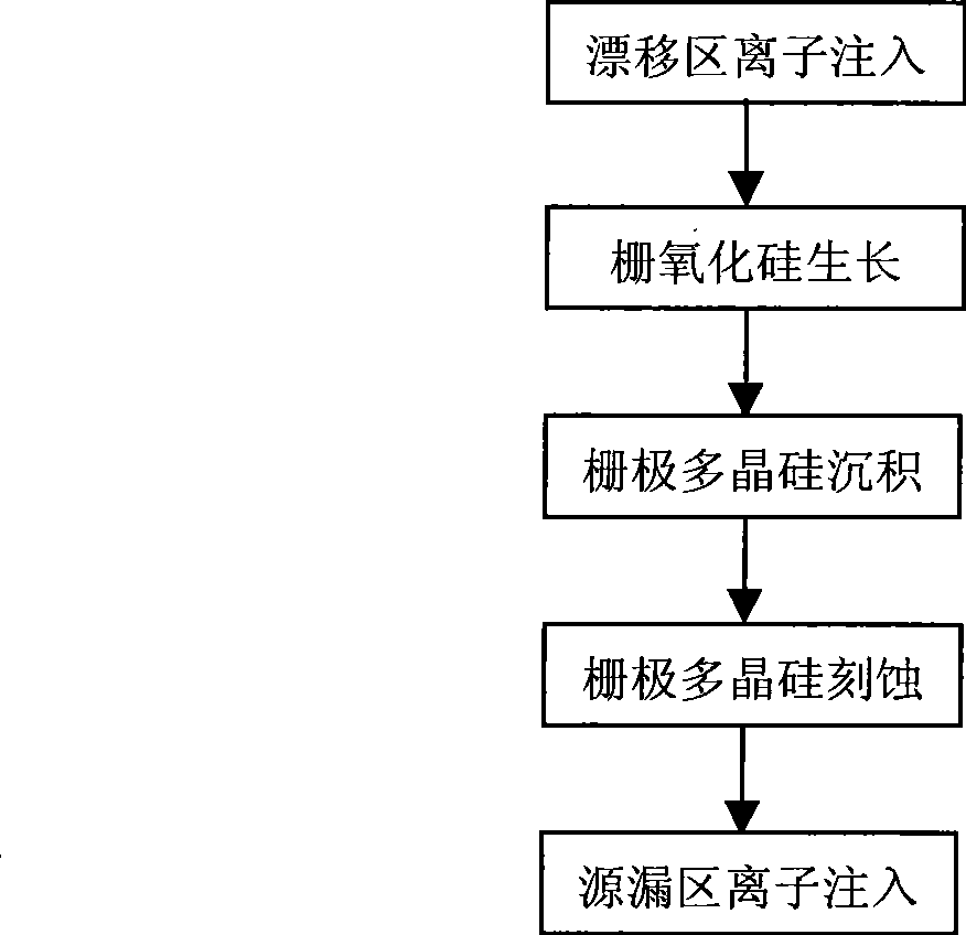
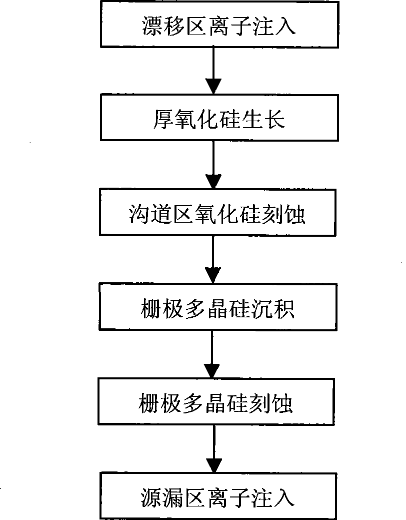
[0026] In one embodiment, such as image 3 Shown, method of the present invention comprises the following steps:

[0027] The first step is to carry out ion implantation on the silicon substrate to form a well region. Those skilled in the art should know that if the transistor to be manufactured is an N-type transistor, the ions to be implanted should be boron ions; The transistor to be manufactured is a P-type transistor, and the ions to be implanted at this time should be phosphorous ions.

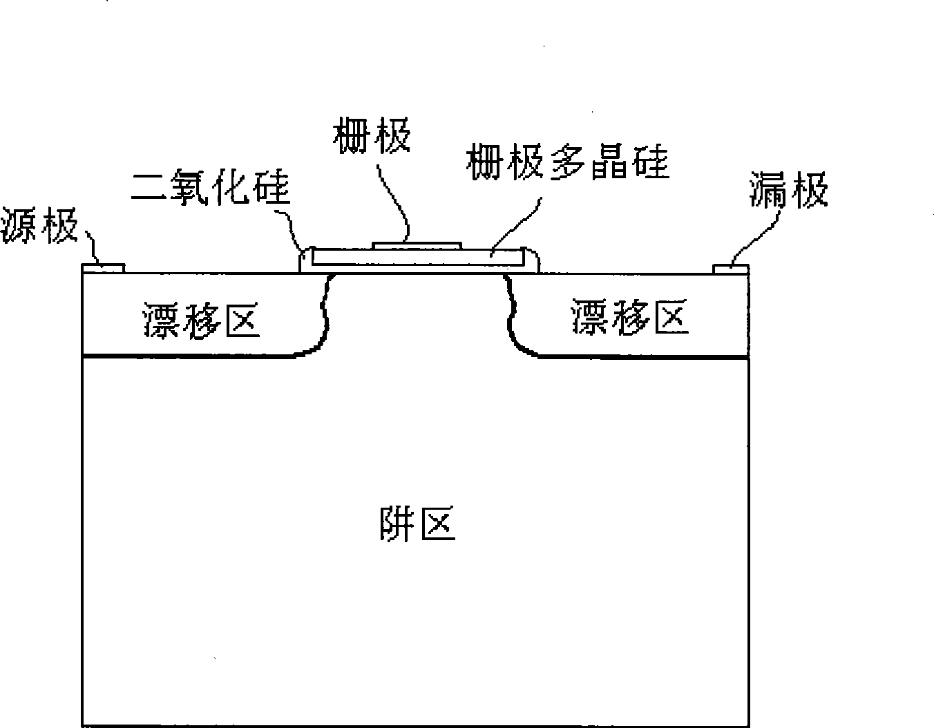
[0028] In the second step, selective ion implantation is performed at the position of the well region of the silicon substrate to form a drift region, and the cross-sectional structure at this time is as follows Figure 4a shown. Those skilled in the art should know that if the transistor to be manufactured is an N-type transistor, the implanted ions should be phosphorus ions at this time; and if the transistor to be manufactured is a P-type transistor, the implanted ions should be fo...


PUM


Abstract

The invention discloses a manufacturing method of a double diffusion field effect transistor, comprising the following steps: greatly increasing the saturation currents of the transistor by increasing the overlapped area of a transistor gate and drift region; changing the electric field distribution on the drift region using an extended grid potential so as to increase breakdown voltages; and synchronously, inhibiting the GIDL effect resulted from the overlapped area using the thick silicon dioxide under the gate at the overlapped area so as to reduce drain currents of transistor. In addition, the method can change the high-voltage breakdown position of the transistor from a transverse junction area to a longitudinal junction area, namely, the high-voltage breakdown position of the transistor is at the strongest junction area, thereby improving the voltage endurance of the double diffusion field effect transistor.

Description

technical field [0001] The invention relates to semiconductor process technology, in particular to a method for manufacturing a double-diffusion field effect transistor. Background technique [0002] For the existing semiconductor process technology, double diffused field effect transistor (Double Diffuse Drain MOS, DDDMOS for short) is a mainstream high-voltage device structure, which is widely used in driver chips and power devices. [0003] Such as figure 1 As shown, in the prior art, the double-diffused transistor is generally manufactured according to the following method: [0004] Firstly, performing ion implantation on the silicon substrate to form a well region, and then performing selective ion implantation in the well region to form a drift region; [0005] Then, growing a gate silicon oxide layer on the well region; [0006] The third step is to deposit a gate polysilicon layer on the gate silicon oxide layer; [0007] The fourth step is to use known photolith...

Claims


Application Information

Patent Timeline
Patent Type & Authority Applications(China)
IPC IPC(8): H01L21/336
Inventor 钱文生刘俊文
Owner SHANGHAI HUA HONG NEC ELECTRONICS
Why Eureka
Try Eureka