Method for enhancing self-aligning contact hole breakdown voltage and polysilicon gate construction

A technology of self-aligned contact holes and polysilicon gates, which is applied in the manufacture of circuits, electrical components, semiconductors/solid-state devices, etc., and can solve the loss of sidewall dielectric materials, the damage of through-hole etching process, and the distance from the top corner of the gate to the through-hole Shrinkage and other issues, to increase the distance, improve the effect of breakdown voltage performance

Active Publication Date: 2009-06-10
SHANGHAI HUAHONG GRACE SEMICON MFG CORP
View PDF0 Cites 6 Cited by
  • Summary
  • Abstract
  • Description
  • Claims
  • Application Information

AI Technical Summary

Problems solved by technology

like Figure 4 As shown, after the self-aligned contact hole etching process, when the alignment process of the self-aligned via hole deviates, the via etching process will damage the top corner of the gate sidewall, resulting in the loss of the sidewall dielectric material , so that the distance between the top corner of the gate and the via hole is reduced

Method used


Image

  • Method for enhancing self-aligning contact hole breakdown voltage and polysilicon gate construction
  • Method for enhancing self-aligning contact hole breakdown voltage and polysilicon gate construction
  • Method for enhancing self-aligning contact hole breakdown voltage and polysilicon gate construction

Examples


Embodiment Construction

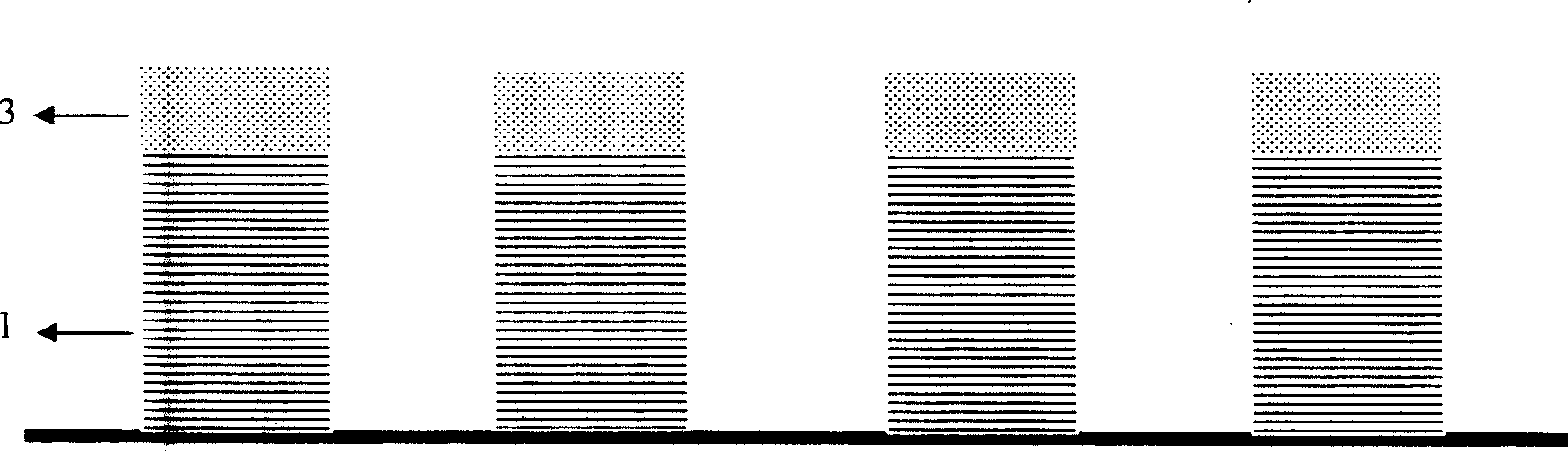
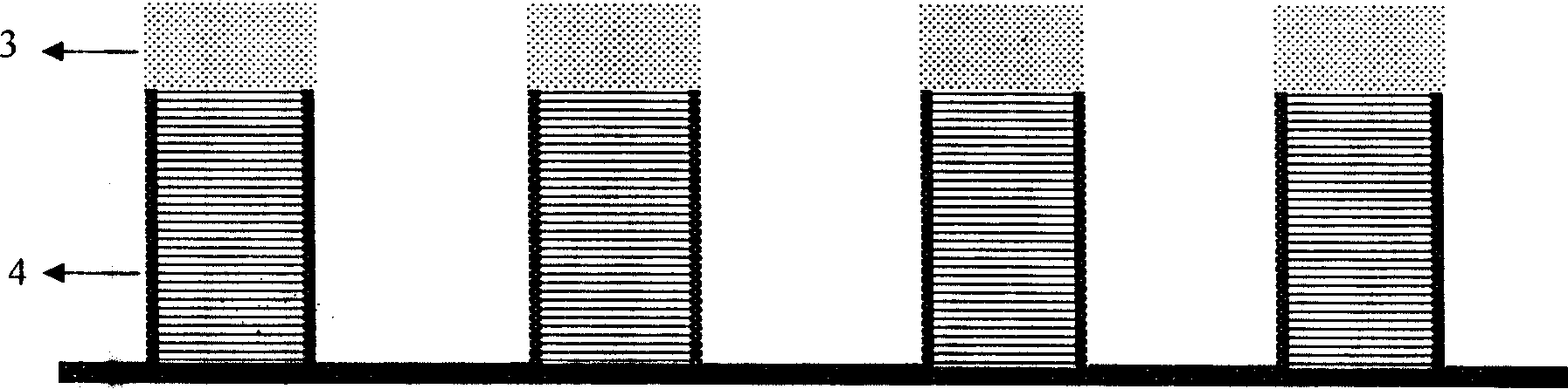
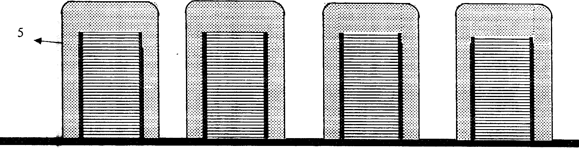
[0017] Such as Figure 5 Shown, the present invention comprises the following steps:

[0018] First, polysilicon, an oxide film and a hard mask layer are sequentially deposited on the oxide layer on the silicon substrate. The hard mask layer is generally a silicon nitride thin film material, and its thickness is generally 300 angstroms to 3000 angstroms. The deposited oxide film is silicon oxide, which can be deposited by high temperature oxide film, chemical vapor deposition oxide film and other methods. The deposited silicon oxide film generally has a thickness of 80 angstroms to 400 angstroms. This layer of oxide film will help to round the top tip of the gate in the subsequent process flow.

[0019] After coating photoresist and photolithography, the hard mask layer, oxide film layer and polysilicon are sequentially etched from top to bottom. During this etching process, plasma etching or chemical wet etching or a combination of plasma etching and chemical wet etching ...


PUM


Abstract

The invention discloses a method for improving breakdown voltage for a self-aligning contact hole, which comprises the following steps: 1, depositing polycrystalline silicon, an oxidation film layer and a hard mask layer on an oxide layer on a silicon substrate in turn; 2, etching the hard mask layer, the oxidation film layer and the polycrystalline silicon from the top down in turn to form a polycrystalline silicon gate, and making a top angle at the top of the polycrystalline silicon become circular; 3, growing an oxidation film layer on the lateral surface of the polycrystalline silicon gate; 4, growing a side wall; and 5, etching the self-aligning contact hole. A polycrystalline silicon structure comprises a polycrystalline silicon layer, the oxidation film layer and the hard mask layer from the bottom up in turn. The oxidation film layer as a polycrystalline silicon gate structure is arranged between the hard mask layer and the polycrystalline silicon layer, the top angle at the top of the polycrystalline silicon gate is made to be circular, and the thicker oxidation film and nitride film are formed at the top angle of the top of the grate, so as to improve the breakdown voltage performance for the self-aligning contact hole.

Description

technical field [0001] The invention relates to the technical field of semiconductor inheritance circuit manufacturing, in particular to a method for improving the breakdown voltage of a self-aligned contact hole, and a polysilicon gate structure for realizing the method. Background technique [0002] The contact hole is a path connecting the front-end device and the back-end wiring, and its breakdown voltage performance is an important electrical parameter of the integrated circuit. In some memory circuits, a self-aligned contact hole process is often utilized to increase circuit density and process window. When the distance between the gate lines is very small or the alignment process of the self-aligned contact hole deviates, the contact hole after optical development will partially sit on the gate spacer layer, and the plasma will Experience a certain amount of damage to the gate sidewall. This reduces the effective distance from the top corner of the gate to the conta...

Claims


Application Information

Patent Timeline
Patent Type & Authority Applications(China)
IPC IPC(8): H01L21/00H01L21/28H01L21/768H01L21/3105H01L21/311H01L29/423
Inventor 迟玉山吕煜坤
Owner SHANGHAI HUAHONG GRACE SEMICON MFG CORP
Why Eureka
Try Eureka