Schottky barrier diode device and manufacturing method thereof

A technology of Schottky potential and diode, which is applied in semiconductor/solid-state device manufacturing, semiconductor devices, electrical components, etc., can solve problems such as incompatibility and complicated manufacturing process, and achieve reduced leakage, simple process steps, and improved reverse The effect of low breakdown voltage

Active Publication Date: 2010-11-03
SHANGHAI HUAHONG GRACE SEMICON MFG CORP
View PDF3 Cites 3 Cited by
  • Summary
  • Abstract
  • Description
  • Claims
  • Application Information

AI Technical Summary

Problems solved by technology

The structure of the existing Schottky diode is basically formed by extending the metal alloy layer such as Ti / W to the N-type epitaxial layer at an appropriate alloy temperature. This device has stable performance and can effectively reduce the saturation voltage drop and improve switching speed, but the manufacturing process of this device is complex and incompatible with ordinary CMOS processes

Method used


Image

  • Schottky barrier diode device and manufacturing method thereof
  • Schottky barrier diode device and manufacturing method thereof
  • Schottky barrier diode device and manufacturing method thereof

Examples


Embodiment Construction

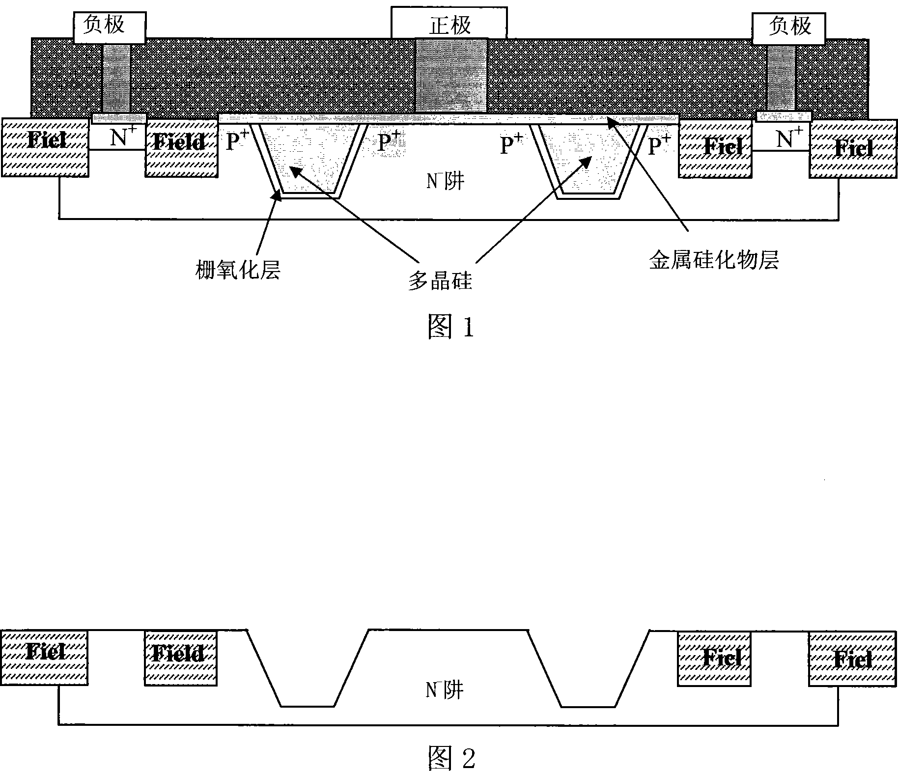
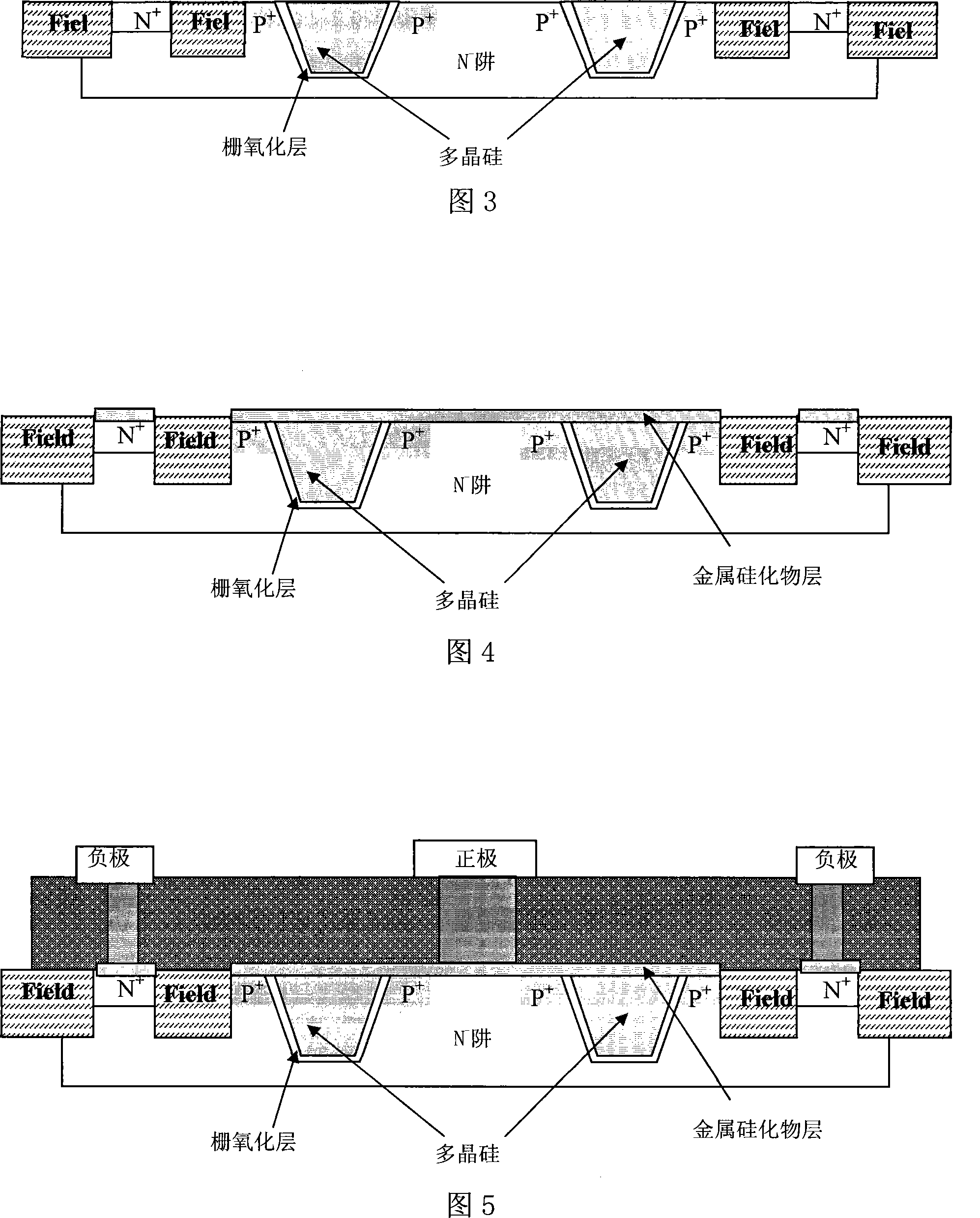
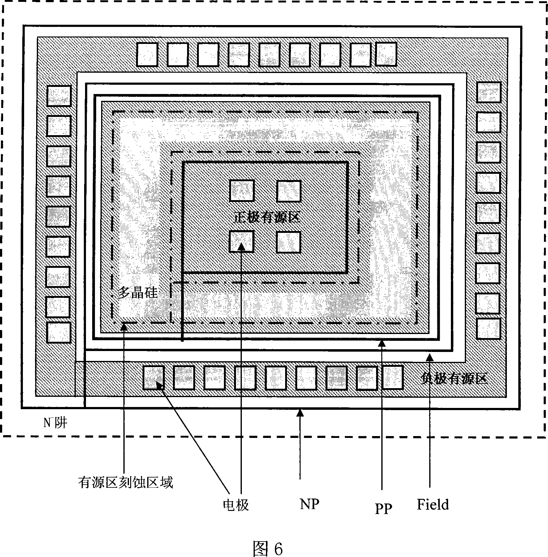
[0016] The invention provides a Schottky barrier diode device, such as figure 1 shown, at N - The well includes a positive active region, a negative active region and an isolation region, the isolation region Field separates the positive active region from the negative active region, and the positive active region includes an annular silicon trench, The silicon trench is filled with polysilicon, and the polysilicon and the N - A gate oxide layer is isolated between the wells, and there are P-type impurity heavily doped regions on both sides of the trench, such as figure 1 Medium P + As shown in the region, the negative active region is a heavily doped region with N-type impurities, such as figure 1 Medium N + As shown in the region, both the positive electrode active region and the negative electrode active region are covered with a metal silicide layer.

[0017] The present invention also provides a method for fabricating the aforementioned Schottky barrier diode device,...


PUM


Abstract

The invention discloses a schottky barrier diode device. An anode active region on an N<-> well comprises an annular silicon groove; the silicon groove is filled with polysilicon; the polysilicon and the N<-> well are isolated with a gate oxide layer; the upper parts of two outer sides of the groove are both provided with a P-type impurity heavily doped region; and the anode active region and a cathode active region are both covered with a metal silicide layer. The invention also discloses a method for manufacturing the schottky barrier diode device. The method comprises the steps of manufacturing an isolation region on the N<-> well, etching the annular silicon groove, growing the gate oxide layer and depositing the polysilicon in turn and performing etching, doping the P-type impurity heavily doped region and the cathode active region, and depositing the metal silicide layers above the anode active region and the cathode active region. The method has simple process steps, accuratelycontrols the contact area with metal silicide by doping P-type impurities beyond a schottky contact region, raises the reverse breakdown voltage of schottky diode, and reduces electric leakage.

Description

technical field [0001] The invention relates to a semiconductor device, in particular to a Schottky barrier diode device. The invention also relates to a method for manufacturing a semiconductor device, in particular to a method for manufacturing a Schottky barrier diode. Background technique [0002] Schottky diode devices are mainly used in the field of high-speed rectification. The structure of the existing Schottky diode is basically formed by extending the metal alloy layer such as Ti / W to the N-type epitaxial layer at an appropriate alloy temperature. This device has stable performance and can effectively reduce the saturation voltage drop and improve Switching speed, but the manufacturing process of this device is complex and incompatible with ordinary CMOS processes. At the same time, the reverse breakdown voltage of the Schottky tube is low, and the leakage current is also a problem that needs to be solved urgently. Contents of the invention [0003] The techni...

Claims


Application Information

Patent Timeline
Patent Type & Authority Patents(China)
IPC IPC(8): H01L29/872H01L21/329
Inventor 过乾
Owner SHANGHAI HUAHONG GRACE SEMICON MFG CORP
Why Eureka
Try Eureka