

Etching stopping layer, semi-conductor device with through hole and forming method thereof
An etch stop layer, semiconductor technology, applied in semiconductor devices, semiconductor/solid-state device manufacturing, semiconductor/solid-state device components, etc., can solve problems such as high resistance, achieve low brightness, reduce resistance, and small lithography lines wide effect
- Summary
- Abstract
- Description
- Claims
- Application Information
AI Technical Summary
Problems solved by technology
Method used
Image

Examples
no. 1 example
[0076] The first embodiment of the present invention proposes a new etch stop layer. figure 2 It is a schematic cross-sectional view of the etching stop layer in the first embodiment of the present invention, as figure 2 As shown, the etch stop layer in this embodiment is divided into two layers—the first etch stop layer 201 and the second etch stop layer 202 located on the first etch stop layer 201 .
[0077] In this embodiment, both the first etch stop layer and the second etch stop layer are titanium nitride layers, but the nitrogen content of the two is different, and the nitrogen content of the second etch stop layer 202 is higher than that of the first etch stop layer 202. Stop layer 201.
[0078] The traditional etch stop layer injects a lot of nitrogen gas during the formation process, which may cause nitriding of the material layer connected to it. For example, when the underlying layer is metal aluminum, the nitrogen gas injected will cause the aluminum to be nitr...
no. 2 example
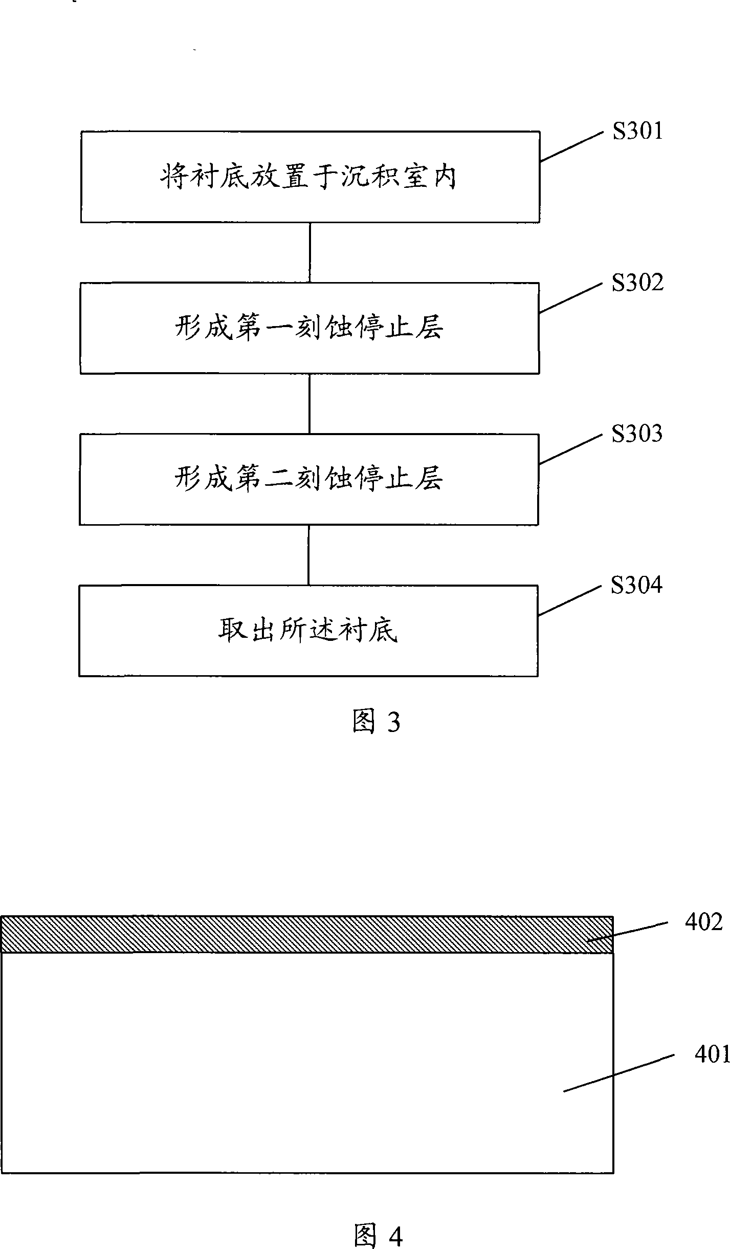
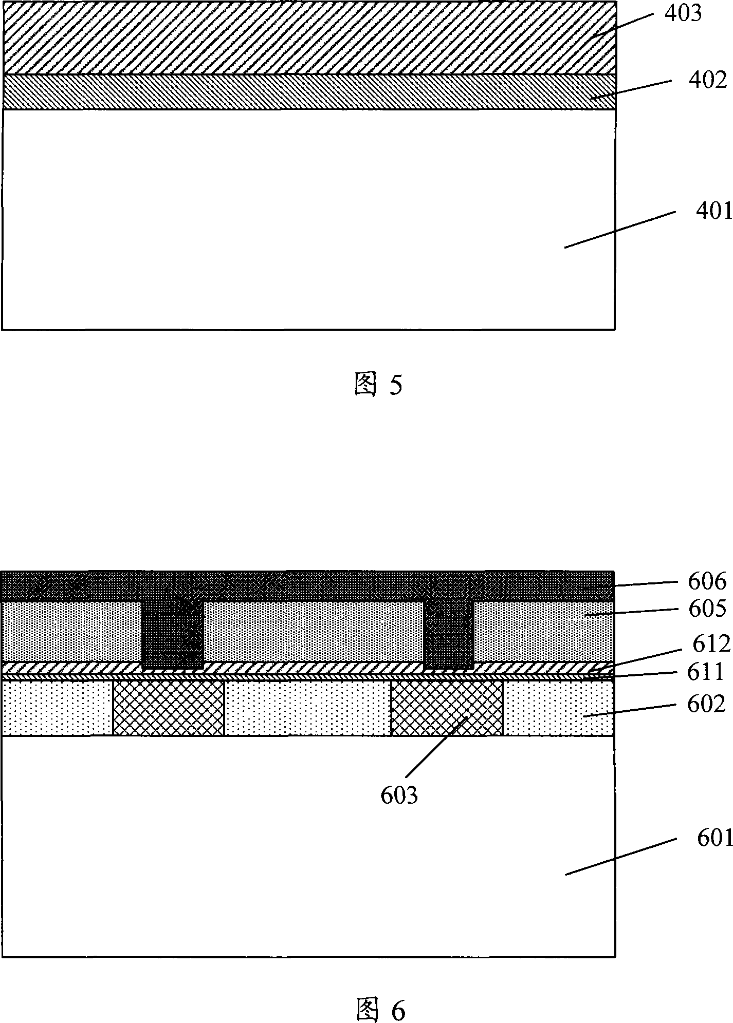
[0083] In this embodiment, a method for forming the etching stop layer in the first embodiment is introduced. image 3 It is a flowchart of a method for forming an etch stop layer according to the second embodiment of the present invention, Figure 4 to Figure 5 In order to illustrate the cross-sectional view of the device of the method for forming the etching stop layer according to the second embodiment of the present invention, the following is combined with Figure 3 to Figure 5 The second embodiment of the present invention will be described in detail.
[0084] Step 301: placing the substrate in a deposition chamber. The etch stop layer in this embodiment is formed by a physical vapor deposition (PVD, Physical Vapor Deposition) method, which uses argon plasma to bombard the titanium target, and the excited titanium ions combine with nitrogen to form titanium nitride Material. It can be considered that the deposition chamber described in this embodiment specifically ref...
no. 3 example
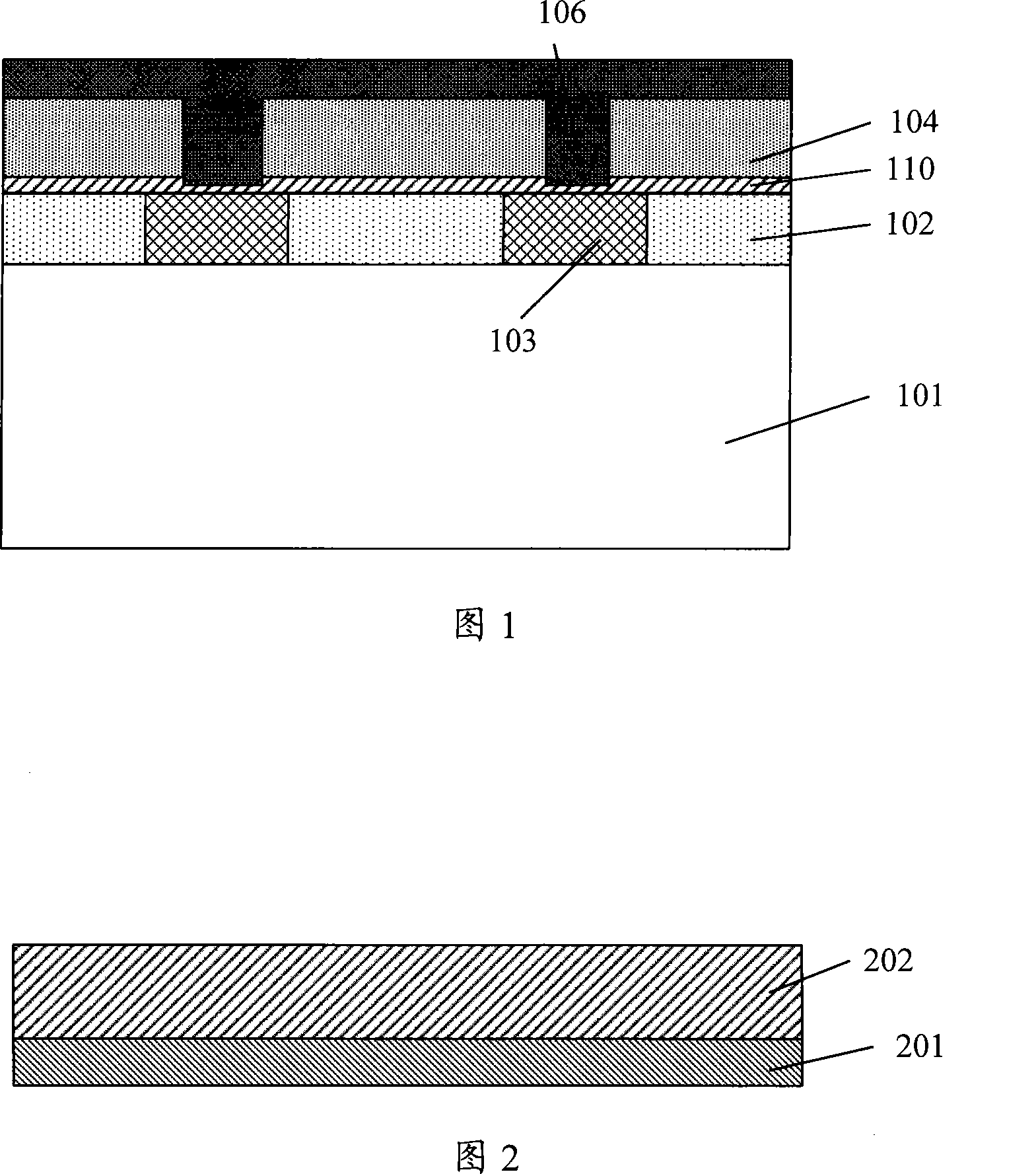
[0108] This embodiment proposes a semiconductor device with a new structure having through holes. Figure 6 It is a schematic cross-sectional view of a semiconductor device with a through hole in the third embodiment of the present invention, as Figure 6 As shown, the semiconductor device with through holes in this embodiment includes a substrate 601, and the substrate 601 has a previous insulating dielectric layer 602, and the previous insulating dielectric layer 602 has a previous metal structure 603 inside, so There is an etch stop layer on the previous insulating dielectric layer 602 and the previous metal structure 603 . The etch stop layer at least includes a first etch stop layer 611, and a second etch stop layer 612 located on the first etch stop layer 611; and the nitrogen content of the second etch stop layer 612 higher than the first etching stop layer 611.
[0109] There is also a latter insulating dielectric layer 605 on the etching stop layer of the two layers...
PUM
 Abstract
Description
Claims
Application Information