

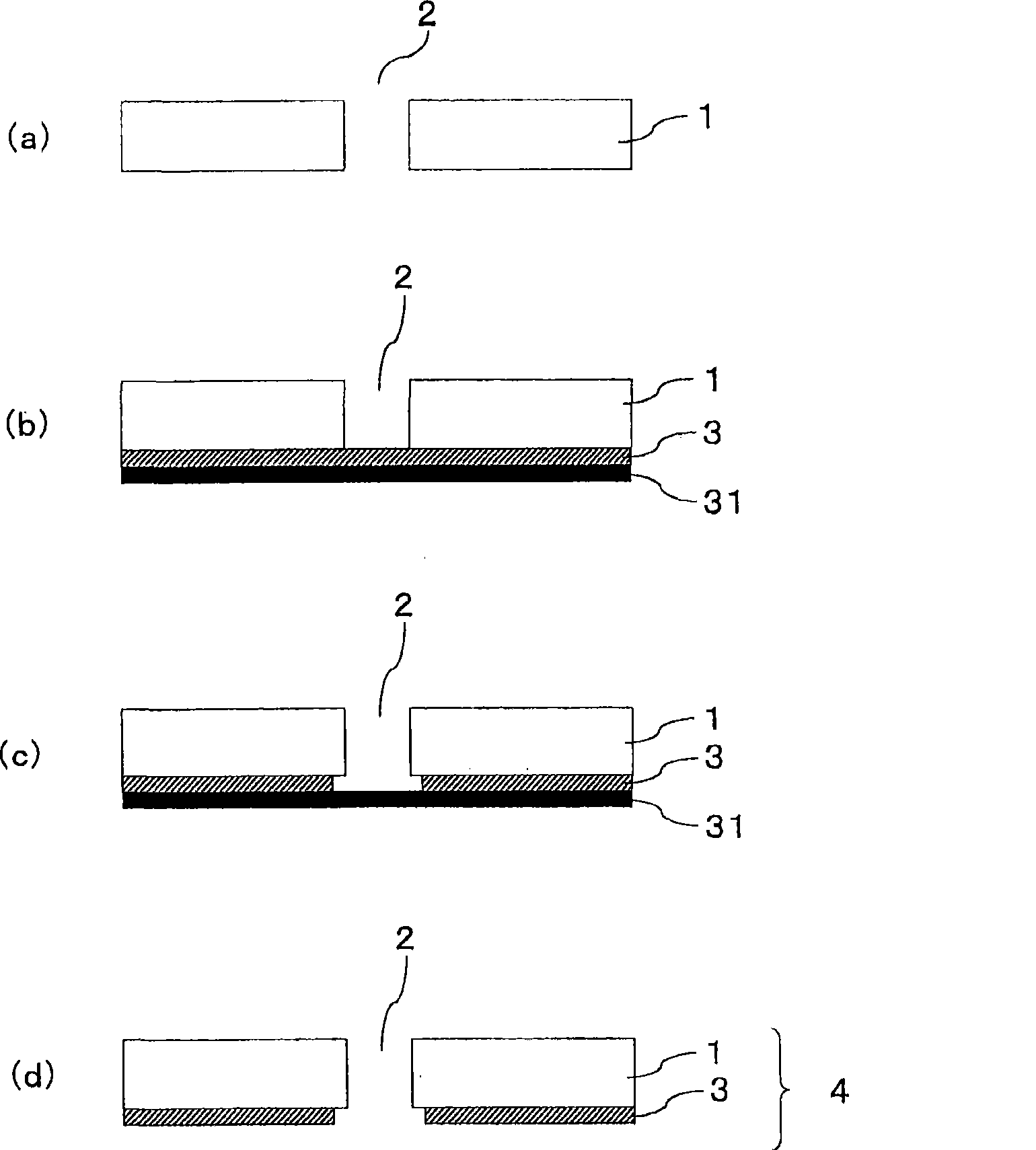
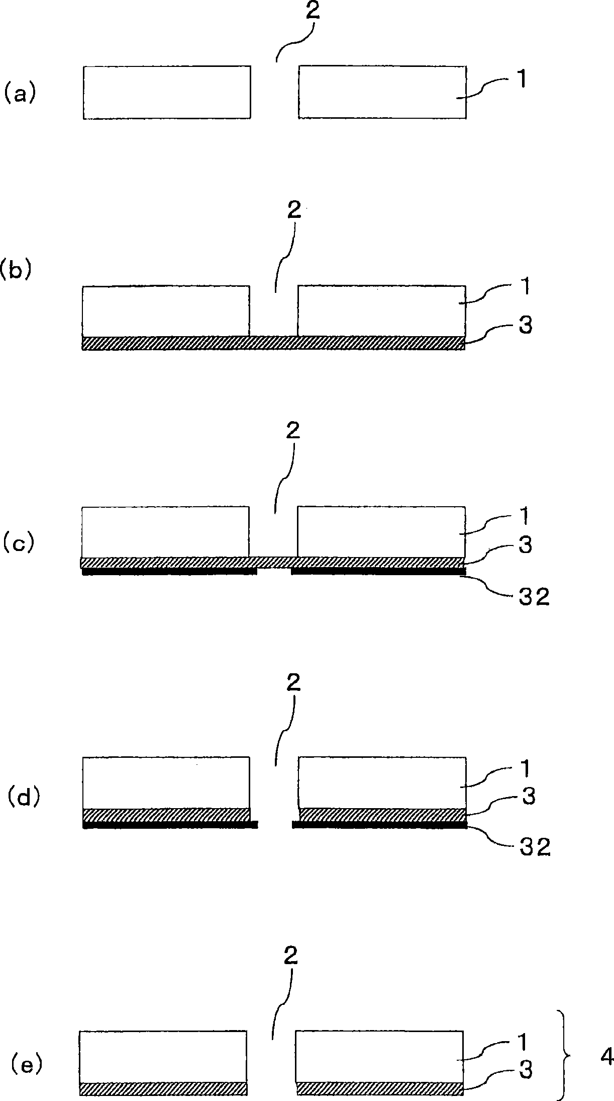
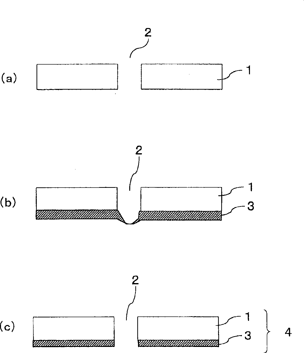
Method for manufacturing screen printing mask with resin, and screen printing mask with resin
A technology of screen printing and manufacturing method, which is applied in the field of the manufacture of the mask for screen printing with resin and the mask for screen printing with resin, can solve the problem of labor and time consumption, smaller opening area, Problems such as the transfer amount of the paste material cannot be obtained, and the effect of improving the adhesion is achieved.
- Summary
- Abstract
- Description
- Claims
- Application Information
AI Technical Summary
Problems solved by technology
Method used
Image

Examples
Embodiment 1
[0184] A SUS 304 stainless steel plate with a plate thickness of 0.2 mm was used as a base material for addition (electroforming), and a photosensitive plated protective layer with a thickness of 100 μm was formed on the surface. Using a photomask provided with a plurality of circular exposure regions with a diameter of 200 μm, pattern exposure and development were performed, thereby forming a cylindrical plating resist with a diameter of 200 μm on the surface of the base substrate. The base substrate forming the plating protection layer is immersed in a nickel sulfamate plating bath at 2A / dm 2 1. Plating was performed under the condition that the bath temperature was 45° C., and a nickel layer with a thickness of 80 μm was formed on the base material except the cylindrical plating resist layer. Then, the plating resist was removed, and the nickel layer was peeled off from the base material to obtain a metal mask including a nickel layer having circular openings by the laminat...
Embodiment 2
[0193] On a stainless steel plate (SUS 304) with a thickness of 80 μm, a number of Figure 19 In the rectangular (200 μm×300 μm) opening shown in (a), a metal mask obtained by a laser method was produced as a mask for screen printing. The radius of curvature Ra of the corner of the rectangular opening was 20 μm. In the same manner as in Example 1, a resin-attached screen printing mask (plate thickness: 100 μm) was produced. However, the treatment time of the resin layer removal liquid a is adjusted so that if Figure 5 The offset width D1 of the straight line portion shown in (a) is 7 μm.
[0194] When the opening of the completed resin-attached screen printing mask was observed with a microscope, no shift in the position of the center of gravity between the screen printing mask and the shape of the opening of the resin layer was observed. Additionally, if Figure 5 The offset width D1 of the straight line portion shown in (a) and (c) is 7 μm, as Figure 5 The offset widt...
Embodiment 3
[0205] A photosensitive etching resist was formed on both surfaces of a SUS 304 stainless steel plate having a plate thickness of 80 μm. Thereafter, using a photomask obtained by inverting the positive and negative of the photomask pattern used in Example 1, pattern exposure was performed on a region other than a circular portion having a diameter of 200 μm. Thereafter, a development treatment was performed to form an etching resist having a circular opening, and then an etching treatment was performed to form a circular opening with a diameter of 200 μm on the stainless steel plate. Then, the etching resist layer was removed, and the metal mask formed by the etching method was obtained as the mask for screen printing. About this metal mask, the formation of the resin layer was performed similarly to Example 1, and the mask for screen printing (board thickness 100 micrometers) with resin was produced. However, the treatment time of the resin layer removing solution a was adju...
PUM
 Abstract
Description
Claims
Application Information