Novel process for electronic element film forming

An electronic component and film-forming technology, which is applied in the direction of electrical components, electrical solid devices, circuits, etc., can solve problems such as pollution, increase indirect man-hours, increase production costs, etc., to solve environmental pollution problems, save production water, and improve production efficiency Effect

Inactive Publication Date: 2009-07-08
NANYANG CITY XINLIJIA ELECTRONICS COMPANY
View PDF0 Cites 1 Cited by
  • Summary
  • Abstract
  • Description
  • Claims
  • Application Information

AI Technical Summary

Problems solved by technology

[0003] 1. Pollution of the environment, affecting the health of workers
The spray liquid contains harmful ingredients such as cadmium, lead, mercury, hexavalent chromium, polybrominated diphenyl ether, and polybrominated biphenyl. pollution within the range, but also affect the health of operating workers
[0004] 2. Low production efficiency, poor controllability of product quality, and large discreteness of products
As far as the production of photoresistors is concerned, for every 1 million substrates invested, about 100 direct production man-hours will be consumed, about 1,000 indirect man-hours will be added, and the scrap rate will be as high as about 30%.
[0005] 3. Serious waste of materials and increased production costs

Method used


Image

  • Novel process for electronic element film forming

Examples


Embodiment Construction

[0016] The specific steps of the new electronic component film forming process of the present invention will be further described in conjunction with the accompanying drawings and examples, and its features and advantages will be clearer.

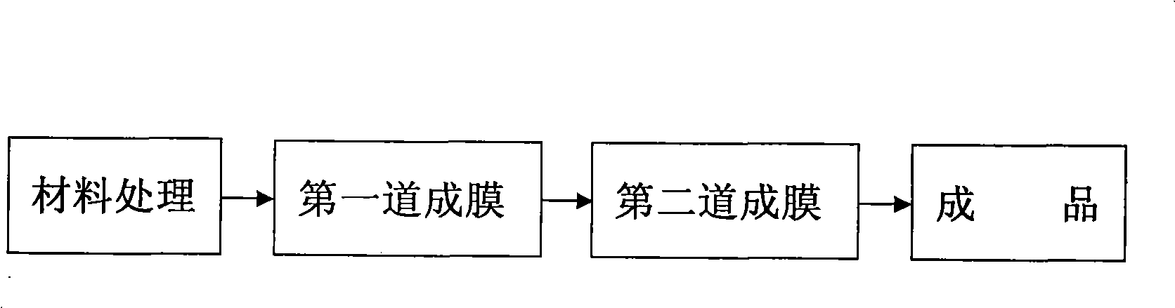
[0017] For an embodiment of the new film-forming process of electronic components of the present invention, see figure 1 , the process steps are: material treatment - first film formation - second film formation - finished product. Among them, the material processing step 1 is to place the mixture of chemical substances that need to be precipitated in a variety of film-forming pharmaceutical materials in a sintering furnace protected by nitrogen gas, and set the temperature and time according to the properties of the material to fully crystallize the pharmaceutical material, and grind it after cooling out of the furnace Form β crystals for later use; in the first film forming step 2, place the electronic component substrate evenly in the co...


PUM


Abstract

The invention relates to an electric component, and researches a novel film forming process of the electric component. The process mainly adopts the steps of the material processing, the first film forming, the second film forming, and the product finishing. Compared with the traditional spray coating method, the process has the advantages that the film layer formed on the electric component is level, compact and uniform; the film forming medicine material is not leaked out and volatilized; the working environment is improved; the waste water and the remaining charge can be reutilized; the problem of environmental pollution is solved; the product quality is guaranteed; the production efficiency is greatly improved; and the production cost is obviously reduced.

Description

technical field [0001] The invention belongs to the field of electronic components, and relates to a film-forming process of electronic components, in particular to a new film-forming process of electronic components. Background technique [0002] In the production process of electronic components, the surface film layer of electronic components has been made by traditional spraying method. Using a special spray gun, the prepared chemical solution is repeatedly sprayed onto the processed electronic component substrate to form a surface film layer. This traditional film-forming method has the following main defects: [0003] 1. Pollution of the environment, affecting the health of workers. The spray liquid contains harmful ingredients such as cadmium, lead, mercury, hexavalent chromium, polybrominated diphenyl ether, and polybrominated biphenyl. Pollution within the range, but also affect the health of operating workers. [0004] 2. Low production efficiency, poor control...

Claims


Application Information

Patent Timeline
Patent Type & Authority Applications(China)
IPC IPC(8): H01L21/50H01L23/06
Inventor 单东林王宁王晓莉
Owner NANYANG CITY XINLIJIA ELECTRONICS COMPANY
Why Eureka
Try Eureka