Method for constructing network on three-dimensional chip

An on-chip network and network structure technology, applied in the direction of data exchange network, digital transmission system, electrical components, etc., can solve the problems of low throughput rate, large network delay, etc., achieve high throughput rate, small network delay, and simple implementation Effect

Inactive Publication Date: 2009-07-15
UNIV OF ELECTRONICS SCI & TECH OF CHINA
View PDF0 Cites 26 Cited by
  • Summary
  • Abstract
  • Description
  • Claims
  • Application Information

AI Technical Summary

Problems solved by technology

[0013] Aiming at the problems of large network delay and low throughput in the existing architecture, the present invention provides a network structure based on De Bruijn graphs, breaks the traditional three-...

Method used


Image

  • Method for constructing network on three-dimensional chip
  • Method for constructing network on three-dimensional chip
  • Method for constructing network on three-dimensional chip

Examples


Embodiment 1

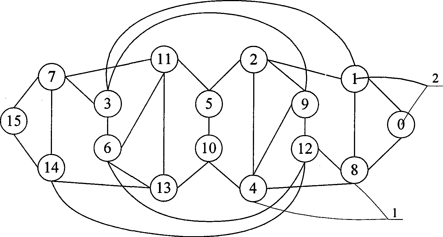
[0035] Network topology: the three-dimensional NoC in Embodiment 1 of the present invention is structured as follows: its horizontal plane network and virtual plane network are both De Bruijn graph structures, and the number of nodes on each horizontal plane network is equal. Each The number of nodes on the virtual plane is also equal. The horizontal number and virtual plane number of each node are arranged according to the construction method of De Bruijn diagram. In order to reduce the complexity of layout and wiring in the chip, the division of nodes that constitute each virtual plane It should be possible to utilize the existing connections on the horizontal network as much as possible. Taking a 4-layer horizontal plane network with 16 nodes on each plane as an example, divide it in the following way: Divide the De Bruijn graph on each horizontal plane network into four Hamiltonian roads each containing 4 nodes, which are respectively recorded as HA, HB, and HC and HD, whe...

Embodiment 2

[0072] The virtual plane division method in this embodiment is: divide all the nodes in the network into two virtual planes, each virtual plane adopts a ring topology. Because there are two imaginary planes, all nodes are connected into two rings, that is, a double ring is formed, and the division of the double ring is carried out as follows:

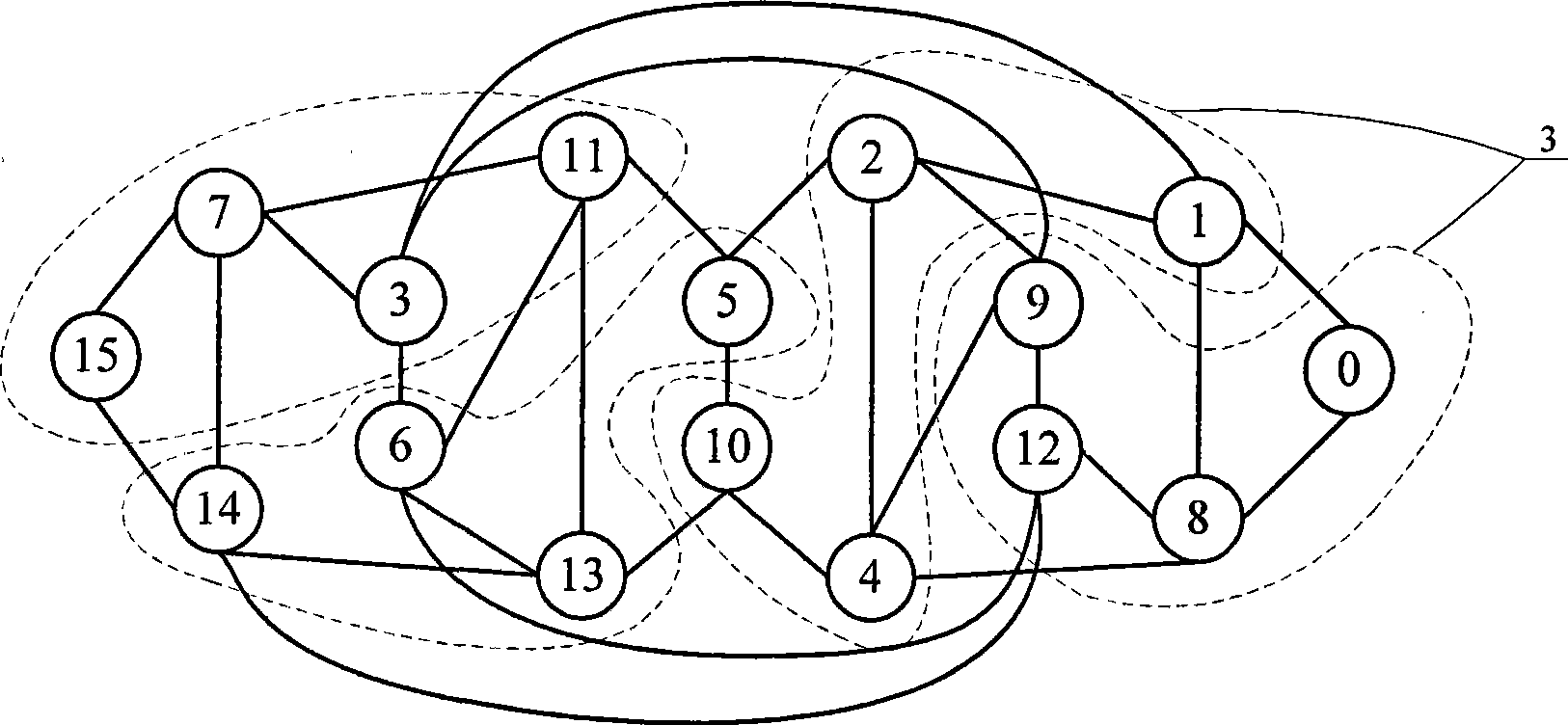
[0073] First, divide all the nodes in the horizontal network of each layer into two Hamilton roads, which are respectively recorded as HA and HB. The starting point and end point of the two roads of HA and HB must be adjacent to each other; The number of nodes of each is N, image 3 It shows a double-ring division method with 16 nodes on each plane, nodes 0, 1, 4, 8, 9, 10, 12 and 13 belong to ring 1, and the remaining nodes belong to ring 2.

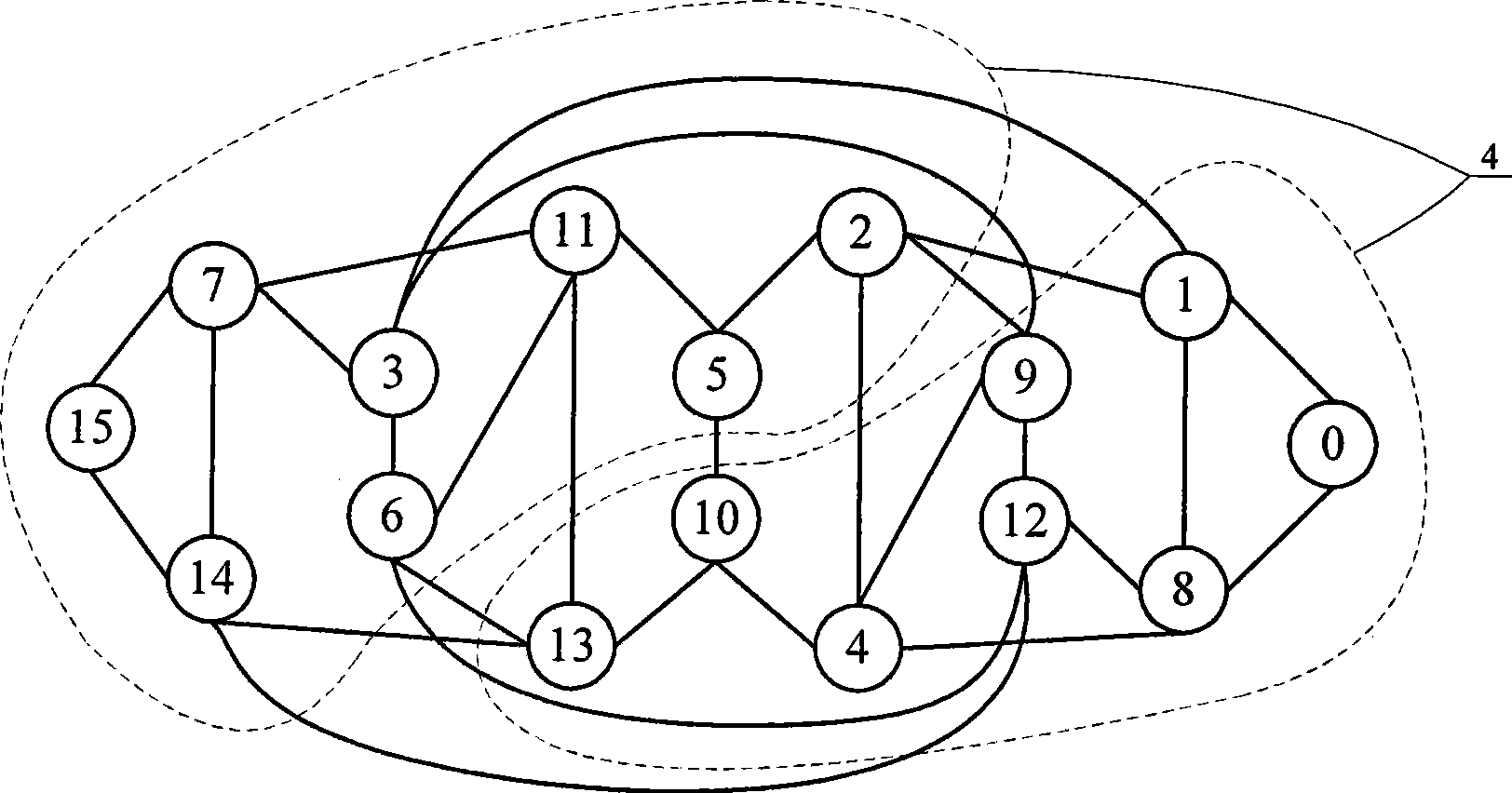
[0074] Then, the HAs of each layer are connected into a ring, and the HBs are connected into another ring, and each ring is a virtual plane. The way each ring is formed is as follows:

[0075]...


PUM


Abstract

The invention provides a three-dimensional network on chip (NoC) structuring method by using a horizontal-plane network structure and a flexible imaginary-plane network structure, wherein, the horizontal-plane network of which the network topology adopts a De Bruijn picture is a plane extending along the X direction and the Y direction; while the imaginary-plane network is a curved surface extending along the three directions of X, Y and Z, the network can be formed by connecting certain nodes of each layer of the horizontal-plane network according to the requirement for solving certain problems such as reducing the wiring complexity or improving the fault-tolerant character, namely, the nodes are not necessarily in a vertical plane. The invention also provides two kinds of imaginary-plane structuring methods comprising a De Bruijn picture structure and a double-ring structure. The first method fully utilizing that the De Bruijn picture allows shorter routing algorithm reduces average hop times in the data transmission, provides a small network delay and has a better fault-tolerant character; the second method improves the transmission efficiency by using the characteristics of low wiring complexity of a ring structure and high data transmission speed and by combining the horizontal-plane network utilizing the advantage of small network diameter of the De Bruijn picture.

Description

technical field [0001] The invention belongs to a network connection method between processing units in an integrated circuit chip, in particular the connection of a three-dimensional on-chip network and the related data transmission process. Background technique [0002] In recent years, with the development of technology, a new form of packaging has emerged—three-dimensional packaging, that is, multiple bare chips are stacked vertically and packaged into a chip. The chip obtained by three-dimensional packaging is called a three-dimensional IC. Compared with the traditional two-dimensional IC, it has many advantages such as large capacity and high density. [0003] Because the architecture of the 3D NoC (Network on Chip) has a great influence on the network throughput, reliability, task mapping of the application layer, and the area and power consumption of the chip, the architecture of the 3D NoC is the most basic solution for realizing the 3D NoC. , the most important li...

Claims


Application Information

Patent Timeline
IPC IPC(8): H04L12/58H04L12/56H04L45/28
Inventor 陈亦欧胡剑浩凌翔符初生
Owner UNIV OF ELECTRONICS SCI & TECH OF CHINA
Why Eureka
Try Eureka