Method for implementing annular cavity whispering gallery mode by photonic crystal structure
A whispering gallery mode and photonic crystal technology, applied in the structure of optical resonant cavity, structure/shape of active medium, laser, etc., can solve problems such as in-depth analysis of mode spectral line characteristics
- Summary
- Abstract
- Description
- Claims
- Application Information
AI Technical Summary
Problems solved by technology
Method used
Image
Examples
Embodiment 1
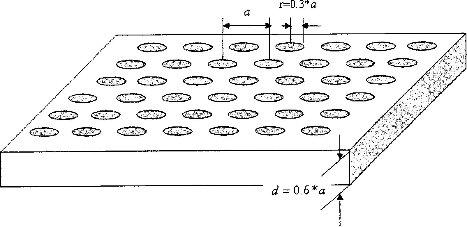
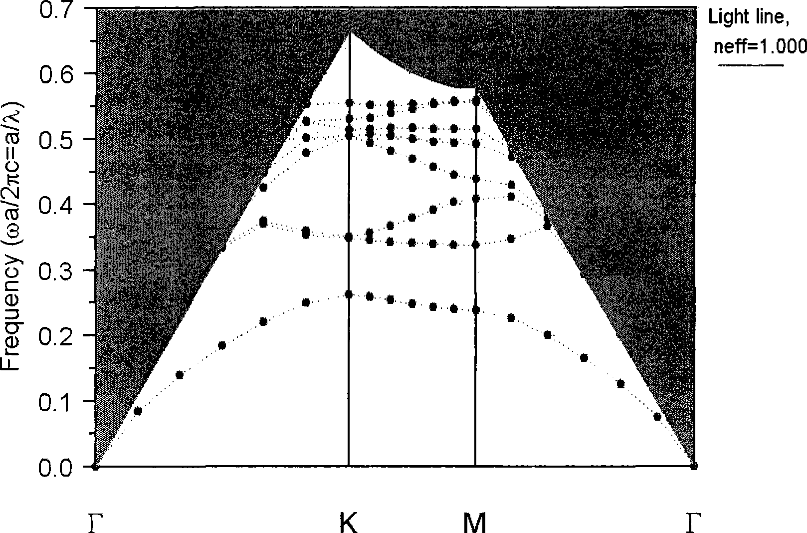
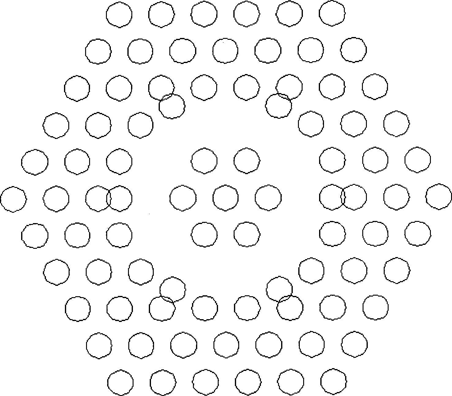
[0047] according to figure 1 The two-dimensional photonic crystal thin plate structure can be realized on the InP material, and its energy band diagram is as follows figure 2 shown, combined with figure 1 and figure 2 ,according to image 3 Photonic crystal structures can be made to realize the whispering gallery mode.
[0048] The parameters of each part are selected as follows:
[0049] Material: InP quaternary semiconductor material with a refractive index of 3.4.
[0050] Photonic crystal structures that can realize whispering gallery modes: in e.g. figure 1 In the complete two-dimensional photonic crystal thin plate structure shown, 12 air holes are removed and six air holes are added at the corners of the photonic crystal ring cavity structure, the structure is as follows Figure 4 As shown, the period of the structure is 470nm, and the radius of the small hole is 141nm. refer to image 3 , during calculation and simulation, the photonic crystal annular cavity ...
Embodiment 2
[0053] according to figure 1 The two-dimensional photonic crystal thin plate structure can be realized on the InP material, and its energy band diagram is as follows figure 2 shown, combined with figure 1 and figure 2 ,according to image 3 Photonic crystal structures can be made to realize the whispering gallery mode.
[0054] Material: InP quaternary semiconductor material with a refractive index of 3.4.
[0055] Photonic crystal structures that can realize whispering gallery modes: in e.g. figure 1 In the complete two-dimensional photonic crystal thin plate structure shown, 12 air holes are removed and six air holes are added at the corners of the photonic crystal ring cavity structure, the structure is as follows Figure 4 As shown, the period of the structure is 470nm, and the radius of the small hole is 141nm. refer to image 3 , during calculation and simulation, the photonic crystal annular cavity is surrounded by 3 layers of photonic crystals (because the thr...
PUM
| Property | Measurement | Unit |
|---|---|---|
| Radius | aaaaa | aaaaa |
Abstract
Description
Claims
Application Information


