Alloying technique for semiconductor chip Au-Si solder

A technology of alloy technology and semiconductor, applied in the direction of metal material coating technology, metal processing equipment, welding/cutting media/materials, etc., can solve the problems of affecting output and reducing the efficiency of bonding chips, and achieve improved yield and short processing time , Fast heating and cooling effect

Active Publication Date: 2009-08-12
深圳深爱半导体股份有限公司
View PDF0 Cites 4 Cited by
  • Summary
  • Abstract
  • Description
  • Claims
  • Application Information

AI Technical Summary

Problems solved by technology

[0004] At present, in the domestic gold-silicon solder eutectic process, the tubular alloy furnace is basically used to alloy the gold-silicon solder. The problem with the alloy in the tubular alloy furnace is that the gold-silicon solder after alloying has no shear force or silicon residue locally. Less, it needs to add friction to stick well when sticking the film, and adding friction will greatly reduce the sticking efficiency and affect the output

Method used


Image

  • Alloying technique for semiconductor chip Au-Si solder
  • Alloying technique for semiconductor chip Au-Si solder
  • Alloying technique for semiconductor chip Au-Si solder

Examples


Embodiment

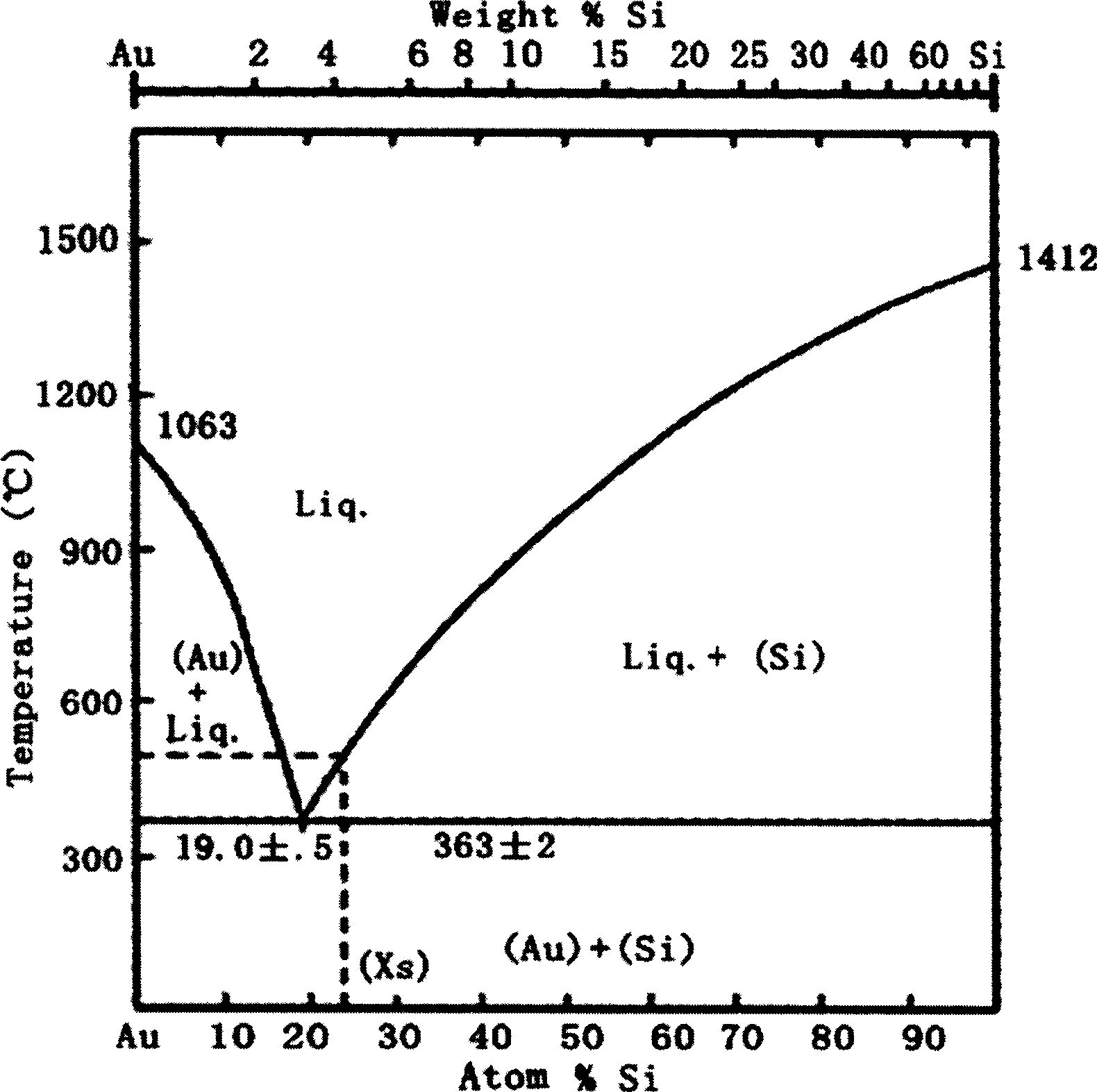
[0028] The above-mentioned silicon wafers were alloyed in a rapid annealing furnace at a temperature of 530°C for 30 seconds. After alloying, the silicon wafers were observed with a metallographic microscope. The pattern on the back side is completely different, and the pattern observed under the 5 times metallographic microscope on the back side of the silicon wafer is # shape (attached Figure 4 ), under a 10x metallographic microscope, only the color of silicon can be seen on the #-shaped lines (attached Figure 5 ), the color of flake silicon will not appear on the whole piece.

[0029] The gold-silicon solder after the alloy is used for trial welding, and the silicon residue can basically reach more than 95%; after the eutectic chip is bonded, the saturation pressure drop and thermal resistance are reduced by about 10%, and the repeatability is very good.

[0030] As can be seen from the above comparative examples and examples, the rapid annealing furnace alloy can thoro...


PUM


Abstract

The invention discloses an alloying process for a semiconductor chip alloyed silicon solder. The alloying process comprises the following steps: S1, carrying out the surface treatment of a silicon slice to be alloyed; S2, coating one or a plurality of metallic layers on the back of the silicon slice subjected to the surface treatment by vaporization on the vacuum condition; and S3, sending the silicon slice coated with the metallic layers into a quick anneal oven for alloy treatment with the temperature of 490 to 550 DEG C and the time of 10 to 50 seconds. The alloying process replaces a conventional tubular type alloying furnace by the quick anneal oven which has the characteristics of accurate temperature control, quick temperature increase and decrease and short processing time in the process. In addition, the application of the quick anneal oven realizes the input and output of a single silicon slice so as to replace the tubular type alloying furnace which has the batch charge and discharge of hundreds of slices each time, make the silicon slice heated evenly, and consequently greatly improve the yield.

Description

【Technical field】 [0001] The invention relates to the technical field of semiconductor device manufacturing technology, in particular to an alloy process of gold-silicon solder for semiconductor chips. 【Background technique】 [0002] After the power transistor chip is manufactured, the collector must be prepared to be packaged into a finished product, and the collector must solve the problem of metal and semiconductor contact. In general, the purpose of metallization on the back of the power transistor chip is to make the collector form a good ohmic contact. The metallized chip on the back has the advantages of small saturation voltage drop (Vcesat), reliable welding, and easy automatic production. There are two processes for the preparation of the collector: the first is the solder process, which uses silver as the solder layer, and solder is added to bond the die and the base; the second is the eutectic process, which uses Solder is a thin layer of alloy, generally gold s...

Claims


Application Information

Patent Timeline
Patent Type & Authority Applications(China)
IPC IPC(8): C23C14/24C23C14/02C23C14/58C23C14/14C23F1/24B23K35/40
Inventor 侯海峰
Owner 深圳深爱半导体股份有限公司
Why Eureka
Try Eureka