Microwave film resistor, microwave film resistor network module and manufacturing method thereof

A resistor network and microwave thin film technology, which is applied in other resistor networks, resistors, non-adjustable metal resistors, etc., can solve the problems of reduced reliability of resistors, large size, and cumbersome attenuator technology

Inactive Publication Date: 2009-09-16
广州翔宇微电子有限公司
View PDF10 Cites 28 Cited by
  • Summary
  • Abstract
  • Description
  • Claims
  • Application Information

AI Technical Summary

Problems solved by technology

However, the manufacturing method of this patent is to form a conductor layer pattern first, and then form a resistance layer in the gap between the conductor layers. There is no resistance layer under the conductor layer, and the conductor layer and the resistance layer are only connected by edge contact parts. It is easy to open the circuit between them. This connection method has poor reliability and cannot meet the requirements of high reliability.
[0006] The patent with the publication number CN101295569A has electrodes on the surface, but it is connected to the internal resistance layer through metallized holes, that is, the entire resistor not only has surface electrodes, but also internal electrodes, which not only increases the length of the metal, thereby increasing The parasitic inductance is eliminated, and the internal electrode is realized through the through hole, the process is complicated, and the reliability of the resistance is reduced
[0007] Publication No. is that the resistor described in th...

Method used


Image

  • Microwave film resistor, microwave film resistor network module and manufacturing method thereof
  • Microwave film resistor, microwave film resistor network module and manufacturing method thereof
  • Microwave film resistor, microwave film resistor network module and manufacturing method thereof

Examples


Embodiment 1

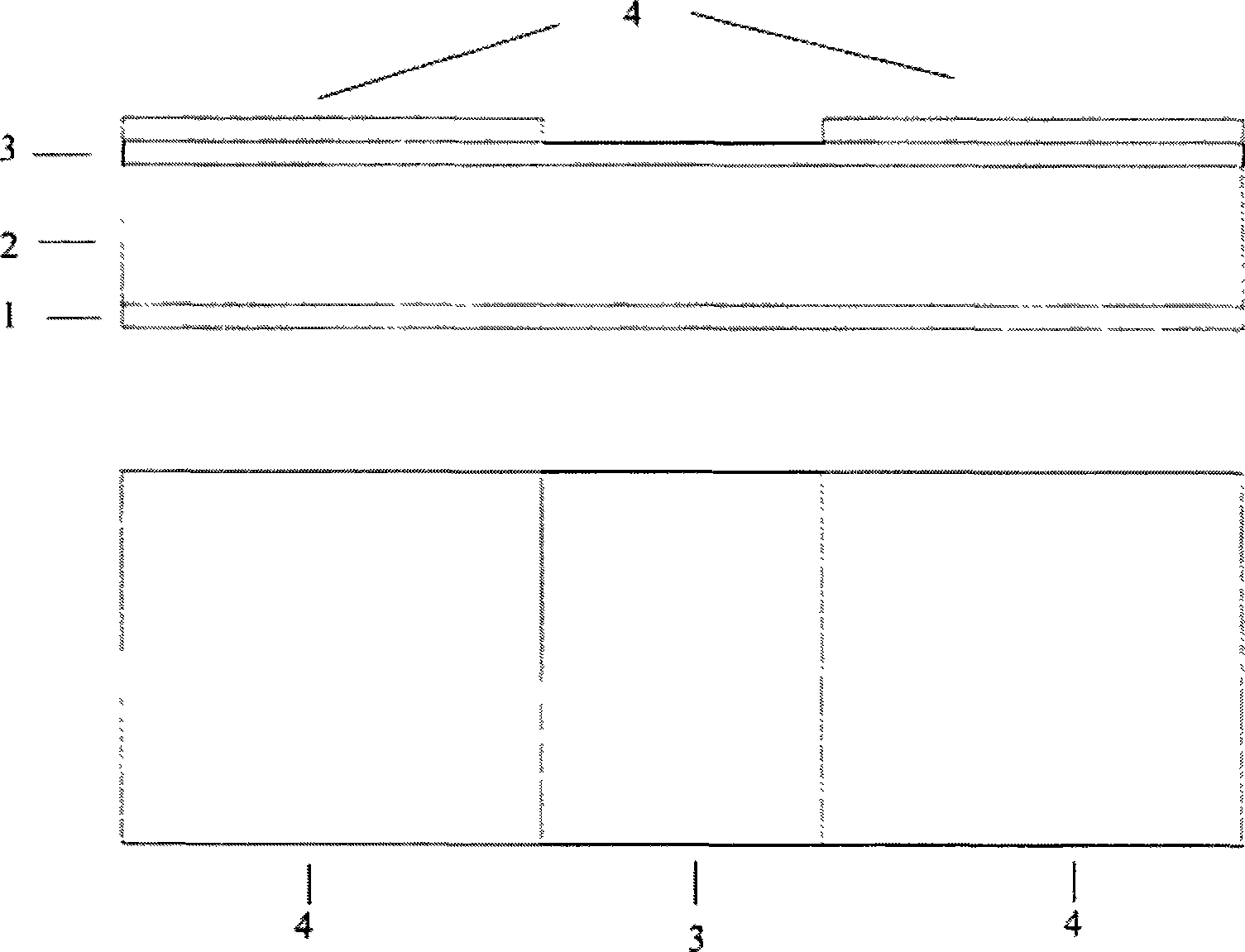
[0080] A layer of TaN thin film was formed on the upper surface of the aluminum oxide substrate with a thickness of 0.381mm and a purity of 99.6% by reactive sputtering, and then Au was sputtered on the surface of the TaN thin film and the lower surface of the ceramic substrate, and then the TaN / Au surface patterning (choose 0201 size mask 1), then thicken the Au layer to 3 μm by electroplating, etch to expose the TaN layer, and finally cut and clean according to the obtained pattern size to obtain the average size of 0201 Thin Film Resistor Products without Sparing, as attached image 3 shown. Or cut and clean the electrode layer and resistance layer according to the obtained graphic size, and the size specification of the metallization layer on the back is 0201 thin film resistors, such as Figure 4 shown. The product was tested after heat treatment at 400°C for 10 minutes, and 98% of the products had a resistance value between 48.5 and 52.0Ω. Calculated according to the ...

Embodiment 2

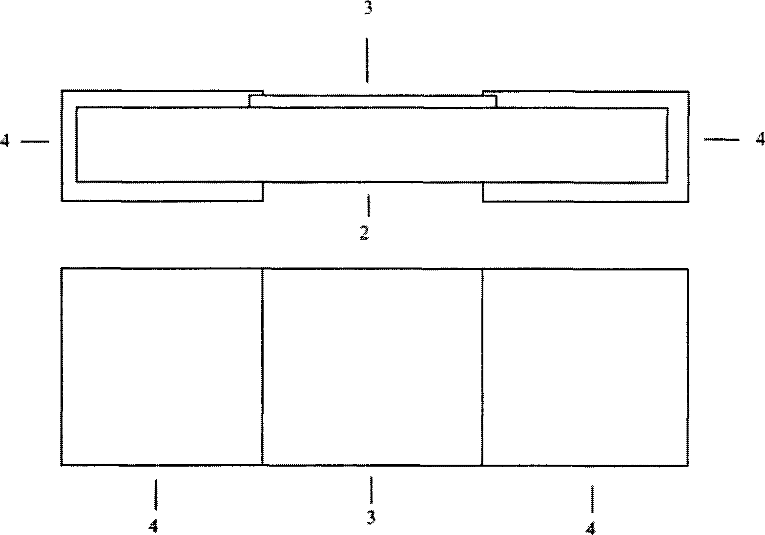
[0082] A layer of NiCr thin film is formed on the upper surface of the aluminum oxide substrate with a thickness of 0.508mm and a purity of 99.6% by reactive sputtering, and then TiW alloy, Ni and Au are sputtered on the NiCr layer and the lower surface of the ceramic substrate, Then pattern the NiCr / TiW / Ni / Au surface (choose 0402 size mask 2), then thicken the Au layer to 4 μm by electroplating, etch to the NiCr layer, and then pattern the NiCr layer (0402 size mask 3 , resistance aspect ratio 2.0:1), corrode to the edge part to expose the ceramic substrate, and finally cut and clean according to the obtained graphic size to obtain the electrode layer, resistance layer and back metallization layer with a size specification of 0402. Thin film resistor products such as Figure 5 shown. Or cut and clean according to the obtained graphic size to obtain a thin film resistor product with a size specification of 0402 electrode layer and resistance layer with no edge left, such as ...

Embodiment 3

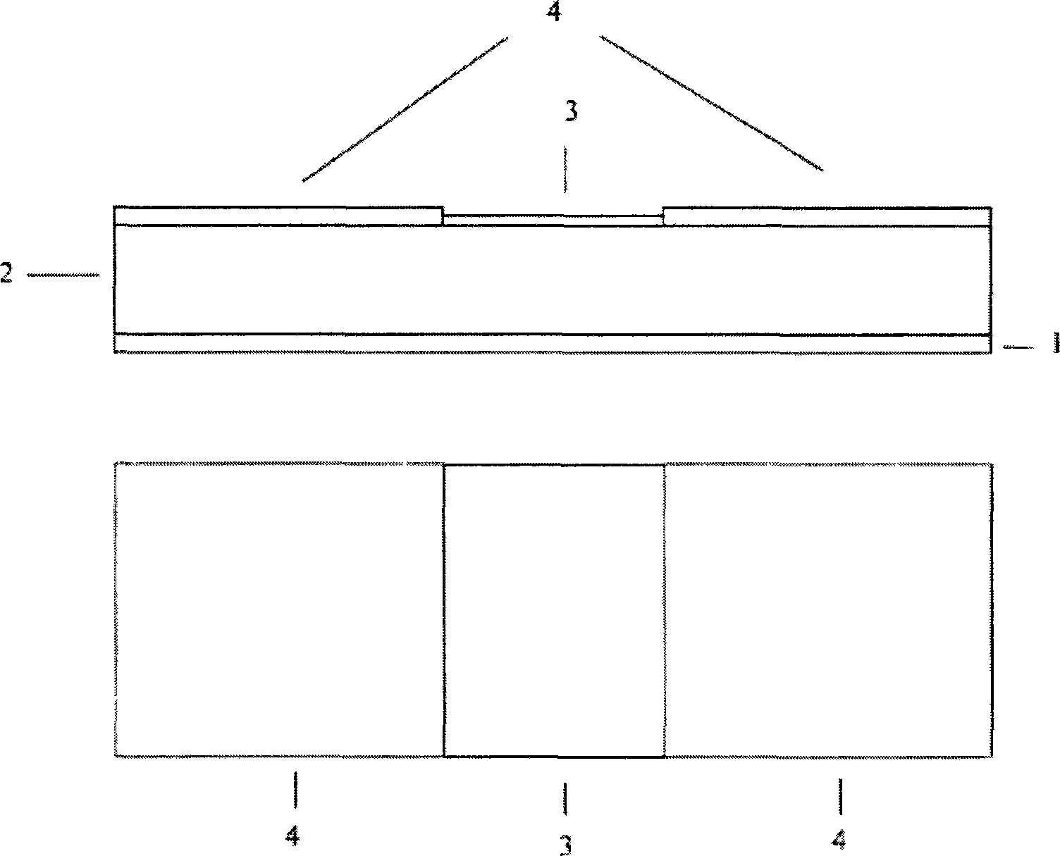
[0084] A layer of TaN film was formed by reactive sputtering on the upper surface of the aluminum nitride substrate with a thickness of 0.381 mm and a purity of 99.6%, and then TiW alloy and Au were sputtered on the lower surface of the TaN film and the ceramic substrate, and then the The surface of TaN / TiW / Au and TiW / Au is patterned (select 0201 size masks 4 and 5), and then the Au layer is thickened to 5 μm by electroplating, and etched until the TaN layer is exposed on the upper surface, and the lower surface is reserved Expose the ceramic layer, then pattern the TaN layer (0201 size mask 6, resistance aspect ratio 1.5:1) and etch until the ceramic substrate is exposed at the remaining part, and finally cut and clean according to the obtained pattern size to obtain the size specification It is a 0201 thin film resistor product, and the electrode layer, resistance layer and back metallization layer of this product have margins, such as Figure 9 shown. The product is heat-t...


PUM

PropertyMeasurementUnit
Thicknessaaaaaaaaaa
Resistanceaaaaaaaaaa
Attenuation valueaaaaaaaaaa

Abstract

The invention discloses a microwave film resistor and a manufacturing method thereof, and belongs to the field of circuit elements. The microwave film resistor comprises a ceramic substrate, a film resistance layer which is adhered to the upper surface of the ceramic substrate and an electrode layer which is adhered to the film resistance layer. The film resistor has the advantages of high precision, high using frequency and high resistance stability. In addition, the invention also discloses a microwave film resistor network module and a manufacturing method thereof, wherein the microwave film resistor network module is formed by integrating three or more microwave film resistors on one module.

Description

technical field [0001] The invention relates to a circuit element, in particular to a microwave thin film resistor and a microwave thin film resistor network module formed by integrating several microwave thin film resistors on a module. [0002] At the same time, the present invention also relates to the manufacturing method of the above microwave thin film resistor and the manufacturing method of the above microwave thin film resistor network module. Background technique [0003] Resistors are one of the most widely used passive components in circuits. They mainly play the roles of power supply decoupling, transistor operating point bias, network matching and interstage coupling in circuits. With the continuous development of electronic products in the direction of high frequency and miniaturization, the resistance element size is required to be smaller and smaller, the frequency of use is higher and higher (above 20GHz), the resistance accuracy and reliability are higher ...

Claims


Application Information

Patent Timeline
IPC IPC(8): H01C7/00H01C17/12H01C17/28H01C1/16
Inventor 程超庄严
Owner 广州翔宇微电子有限公司
Why Eureka
Try Eureka