Pixel structure of thin film transistor-liquid crystal display and manufacturing method thereof

A thin-film transistor and liquid crystal display technology, which is applied in the direction of transistor, semiconductor/solid-state device manufacturing, electric solid-state device, etc., can solve problems such as space that does not improve the display effect of TFT-LCD, over-cut open circuit, residual short circuit of TFT channel, etc.

Active Publication Date: 2009-09-30
K TRONICS (SUZHOU) TECH CO LTD +1
View PDF0 Cites 23 Cited by
  • Summary
  • Abstract
  • Description
  • Claims
  • Application Information

AI Technical Summary

Problems solved by technology

[0010] Although the current 4mask design process of TFT-LCD pixel structure improves the production capacity of TFT-LCD, it still cannot meet the growing market demand
The existing source-drain planar channel structure is formed by using the gray-tone masking process or the half-tone masking process in the second masking process. Due to the unstable pr...

Method used


Image

  • Pixel structure of thin film transistor-liquid crystal display and manufacturing method thereof
  • Pixel structure of thin film transistor-liquid crystal display and manufacturing method thereof
  • Pixel structure of thin film transistor-liquid crystal display and manufacturing method thereof

Examples


Embodiment Construction

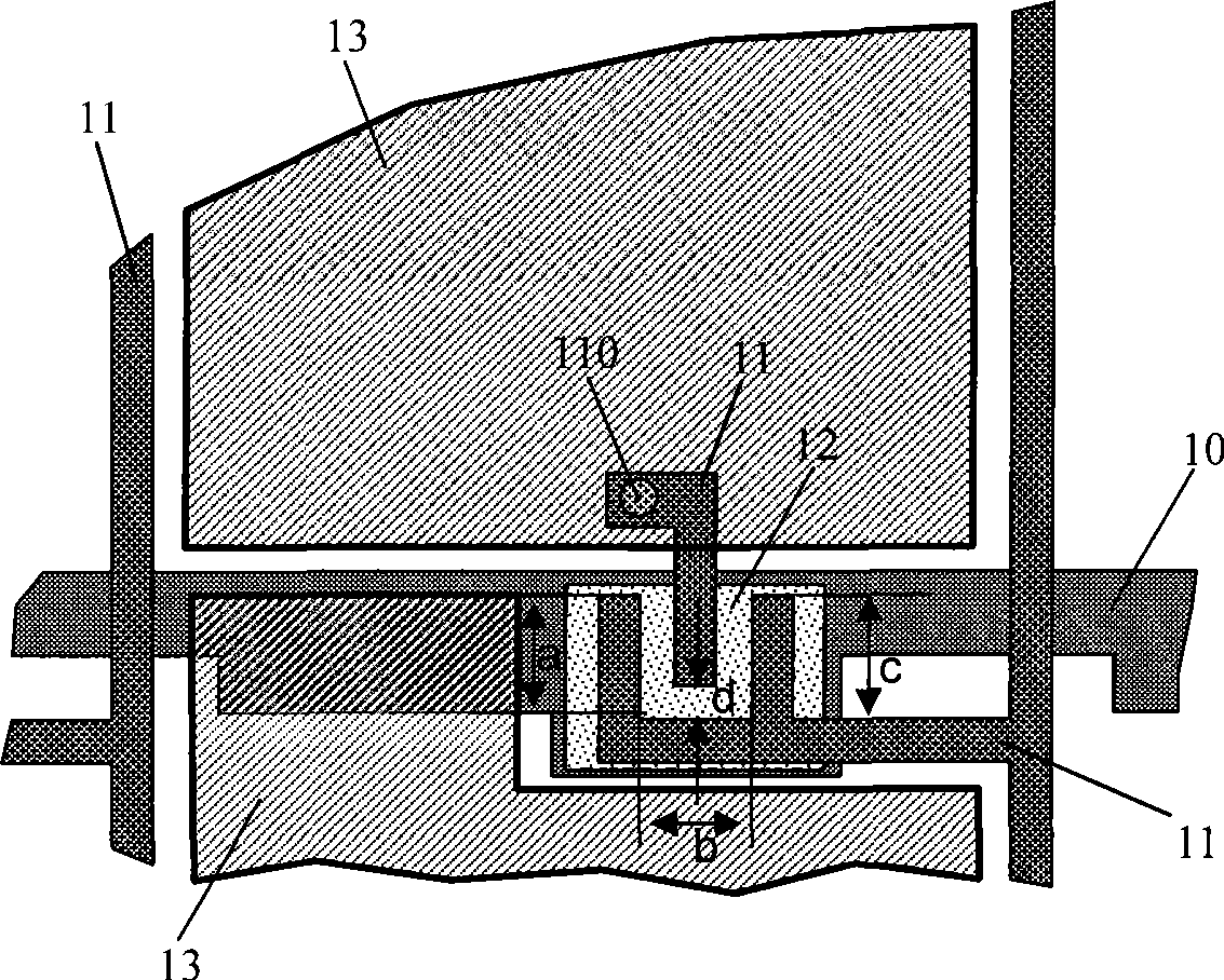
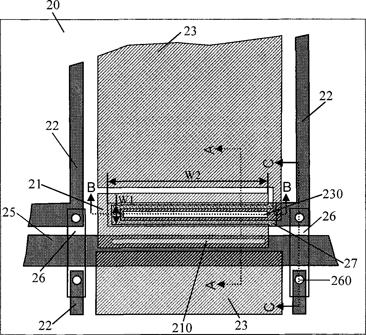
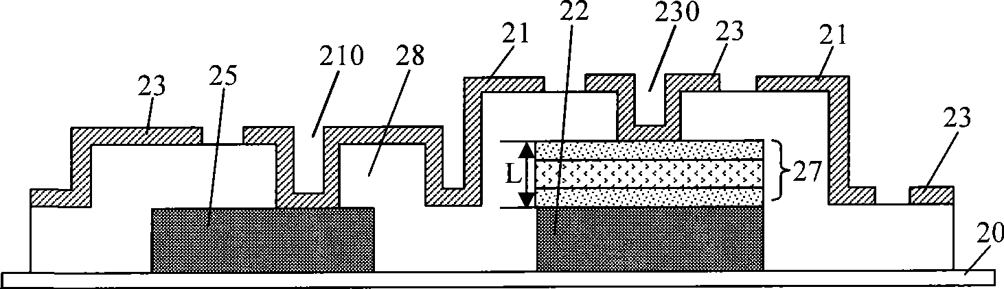
[0041]The present invention provides a pixel structure of a thin film transistor liquid crystal display, which includes a gate line and a data line, and a gate line and a data line cross to define a pixel area, and each pixel area includes at least one thin film transistor and a pixel electrode, wherein the thin film The source of the transistor is formed on the bottom layer, on which are the doped semiconductor layer, the semiconductor layer, the doped semiconductor layer and the drain, the source of the thin film transistor is connected to the data line, and the drain is connected to the pixel electrode; the gate of the thin film transistor The electrodes are formed on the doped semiconductor layer, the semiconductor layer, and the side surfaces of the doped semiconductor layer, and are connected to the gate lines. The thin film transistor with pixel structure of the present invention forms a vertical TFT channel because the gate is formed on the side of the active layer (dop...


PUM


Abstract

The invention discloses a pixel structure of a thin film transistor-liquid crystal display and relates to a TFT-LCD technology, which is provided aiming to solve the problems of poor display effect and complex process of the current TFT-LCD. The invention adopts the technical scheme that the pixel structure comprises a grid line and a data line, wherein the grid line and the data line are intercrossed to form a pixel area, the pixel area comprises at least one thin film transistor and a pixel electrode, the source electrode of the thin film transistor is formed at the bottom layer, an active layer and a drain electrode are arranged on the source electrode in sequence, the source electrode is connected with the data line and the drain electrode is connected with the pixel electrode; the grid is formed on the side surface of the active layer and is connected with the grid line; and the side surface of the active layer and the grid part opposite to the side surface of the active layer form a vertical current channel, i.e., a side grid channel is formed. The invention also discloses a manufacturing method of the pixel structure. The invention obviously enhances the current intensity of the TFT channel, improves the display effect of the TFT-LCD and improves the manufacturing efficiency of the pixel structure of the TFT-LCD.

Description

technical field [0001] The invention relates to thin film transistor liquid crystal display (TFT-LCD, Thin Film Transistor-Liquid Crystal Display) technology, in particular to a pixel structure of a thin film transistor liquid crystal display and a manufacturing method thereof. Background technique [0002] In recent years, TFT-LCD has dominated the current flat panel display market due to its advantages of small size, light weight, low power consumption and no radiation. The TFT-LCD display screen is composed of an array glass substrate and a color film glass substrate, and the liquid crystal material is sealed after vacuuming. The TFT-LCD display forms an array of hundreds of thousands to millions of pixels, and each pixel displays images through the control of TFT. [0003] figure 1 It is an enlarged schematic diagram of the existing thin film transistor liquid crystal display pixel structure, such as figure 1 As shown, the pixel structure of the existing thin film tra...

Claims


Application Information

Patent Timeline
IPC IPC(8): G02F1/1362H01L27/12H01L29/786H01L21/84G03F1/00G03F1/32
CPCH01L27/124
Inventor 何祥飞王威
Owner K TRONICS (SUZHOU) TECH CO LTD
Why Eureka
Try Eureka