
Method for preparing point contact electrode at back of solar cell by utilizing laser induced thermit reaction
A backside point contact and thermite reaction technology, applied in the field of solar energy, can solve the problems of reducing battery short-circuit current, failure to form ohmic contact, material damage, etc., to increase short-circuit current and open-circuit voltage, reduce carrier recombination rate, reduce The effect of small damage
- Summary
- Abstract
- Description
- Claims
- Application Information
AI Technical Summary
Problems solved by technology
Method used
Image

Examples
Embodiment Construction
[0018] The method for preparing a point-contact electrode on the back of a solar cell by using laser-induced thermite reaction provided by the present invention comprises the following steps:
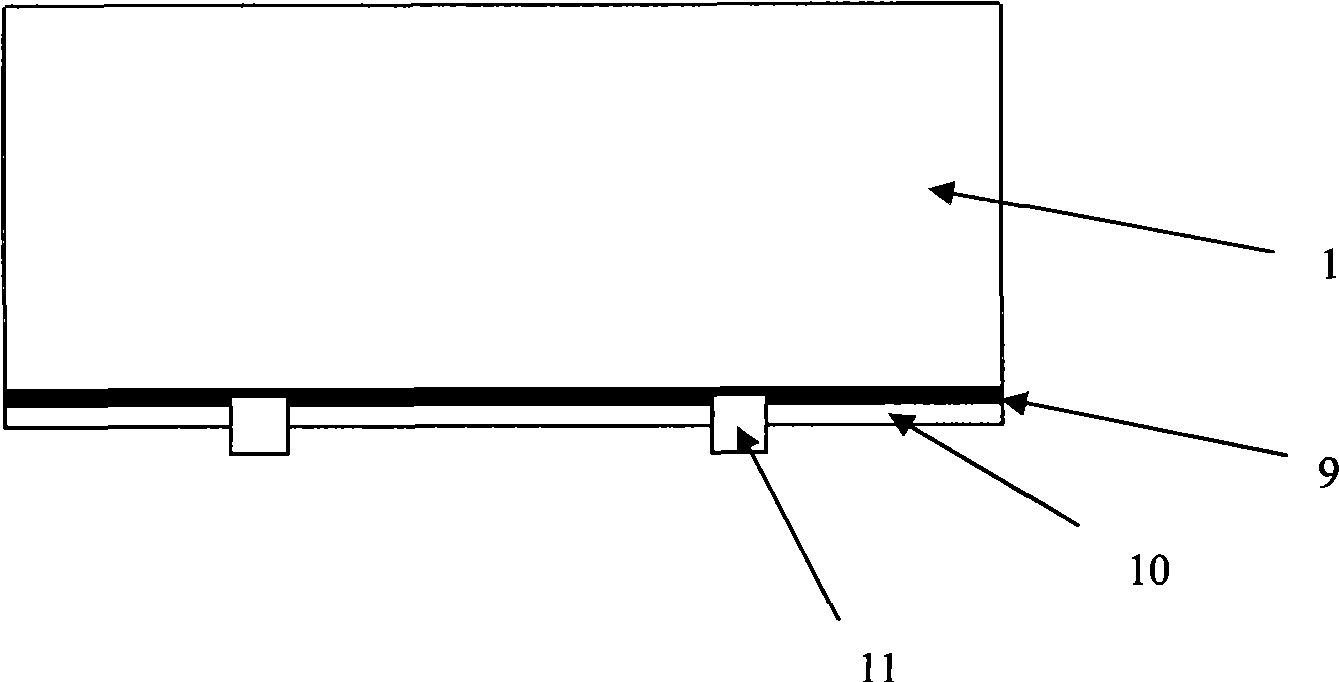
[0019] (1) The front surface of the silicon substrate 1 is cleaned and textured, diffused to obtain the front surface emission junction region 9, and the front surface anti-reflection film 10 (such as SiNx: H or SiO 2 etc.), prepare the front silver grid line electrode 11, such as figure 1 shown;
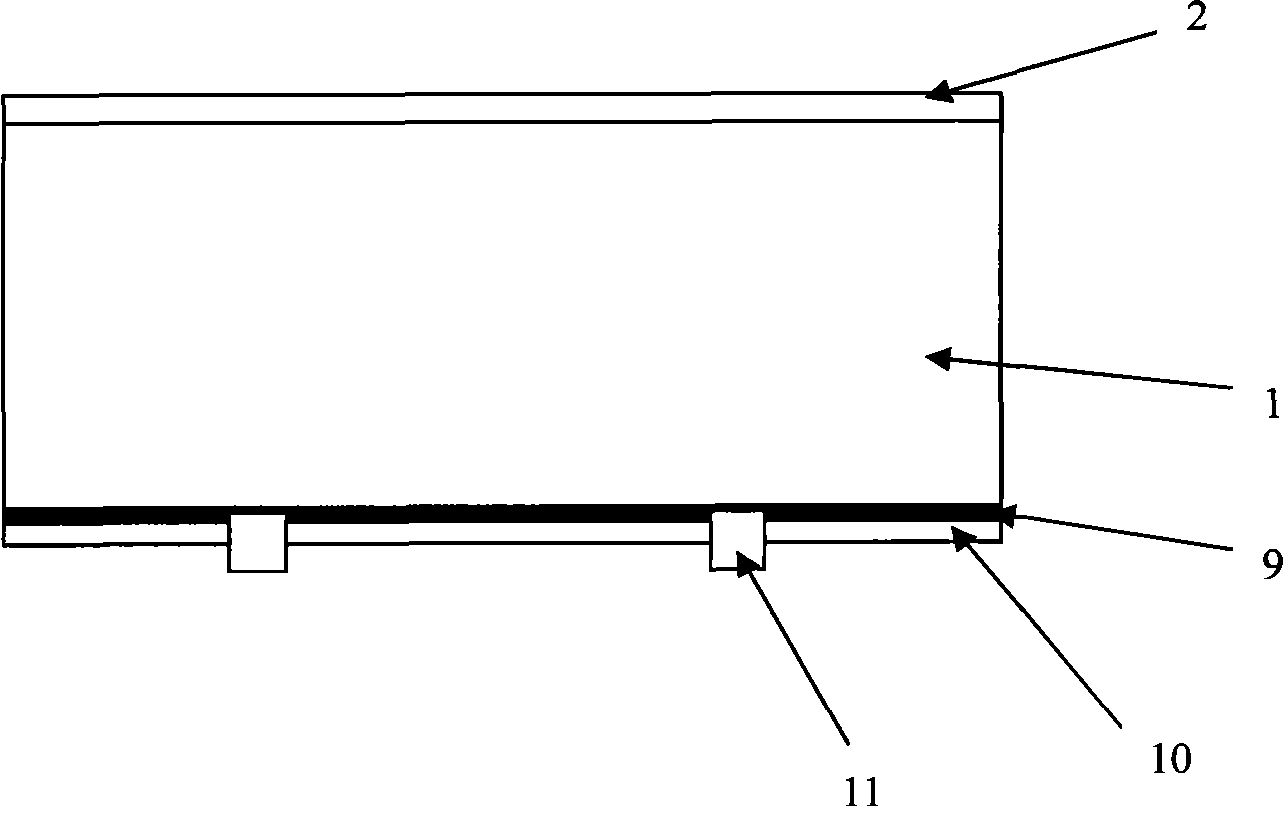
[0020] (2) Coating a layer of passivation dielectric layer (2) (such as SiNx: H or SiO on the back side of silicon substrate 1 2 etc.), such as figure 2 shown;
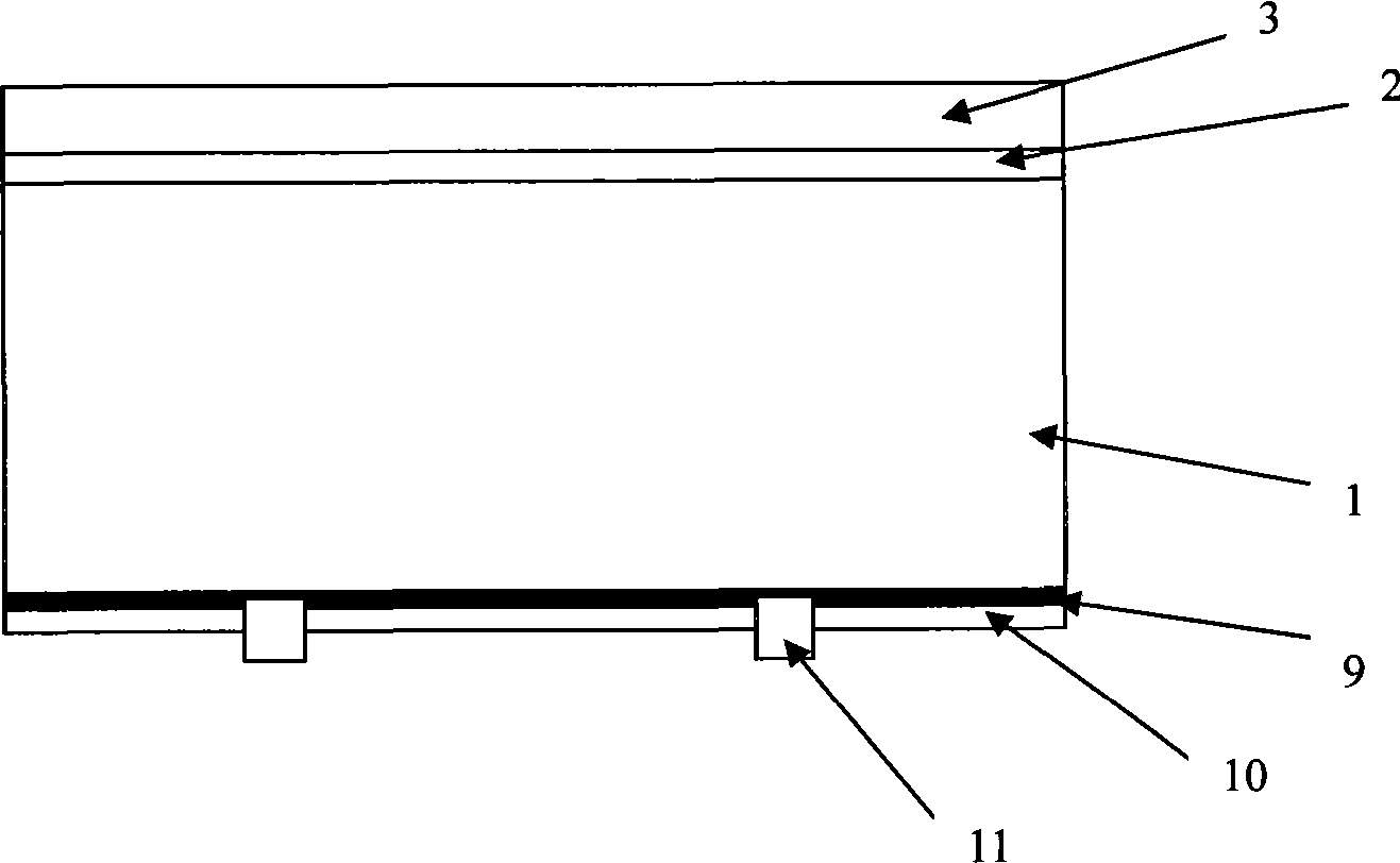
[0021] (3) A layer of aluminum layer 3 is vapor-deposited on the passivation medium layer 2, the thickness of the aluminum layer 3 is 0.1-10um, such as image 3 shown;
[0022] (4) Printing or coating dot-shaped thermite 4 arranged in a certain array on the aluminum layer 3, such as Figure 4 shown;
[0023] (5) Ignite therm...
PUM
 Abstract
Description
Claims
Application Information