
Analysis chip and analysis method

A chip and substance technology, applied in the field of analytical chips, can solve the problems of air bubble obstruction, difference in detection sensitivity, residual air bubbles, etc., and achieve the effect of suppressing residue, high sensitivity, and preventing agglomeration

Inactive Publication Date: 2009-11-11
TORAY IND INC
View PDF5 Cites 15 Cited by
  • Summary
  • Abstract
  • Description
  • Claims
  • Application Information

AI Technical Summary

Problems solved by technology

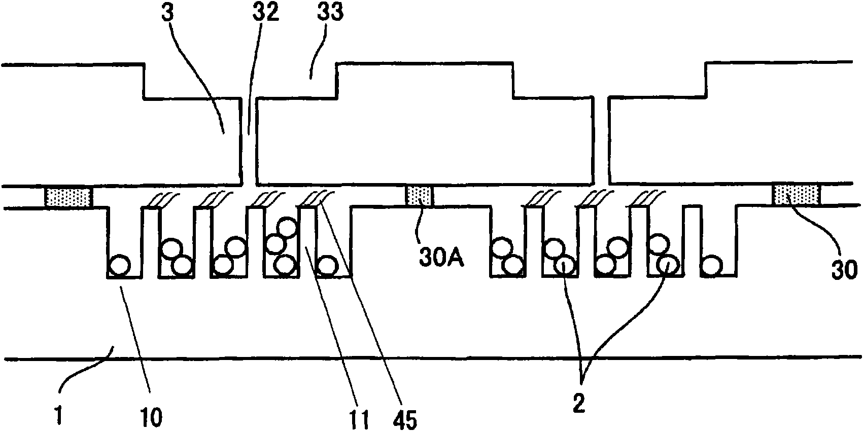
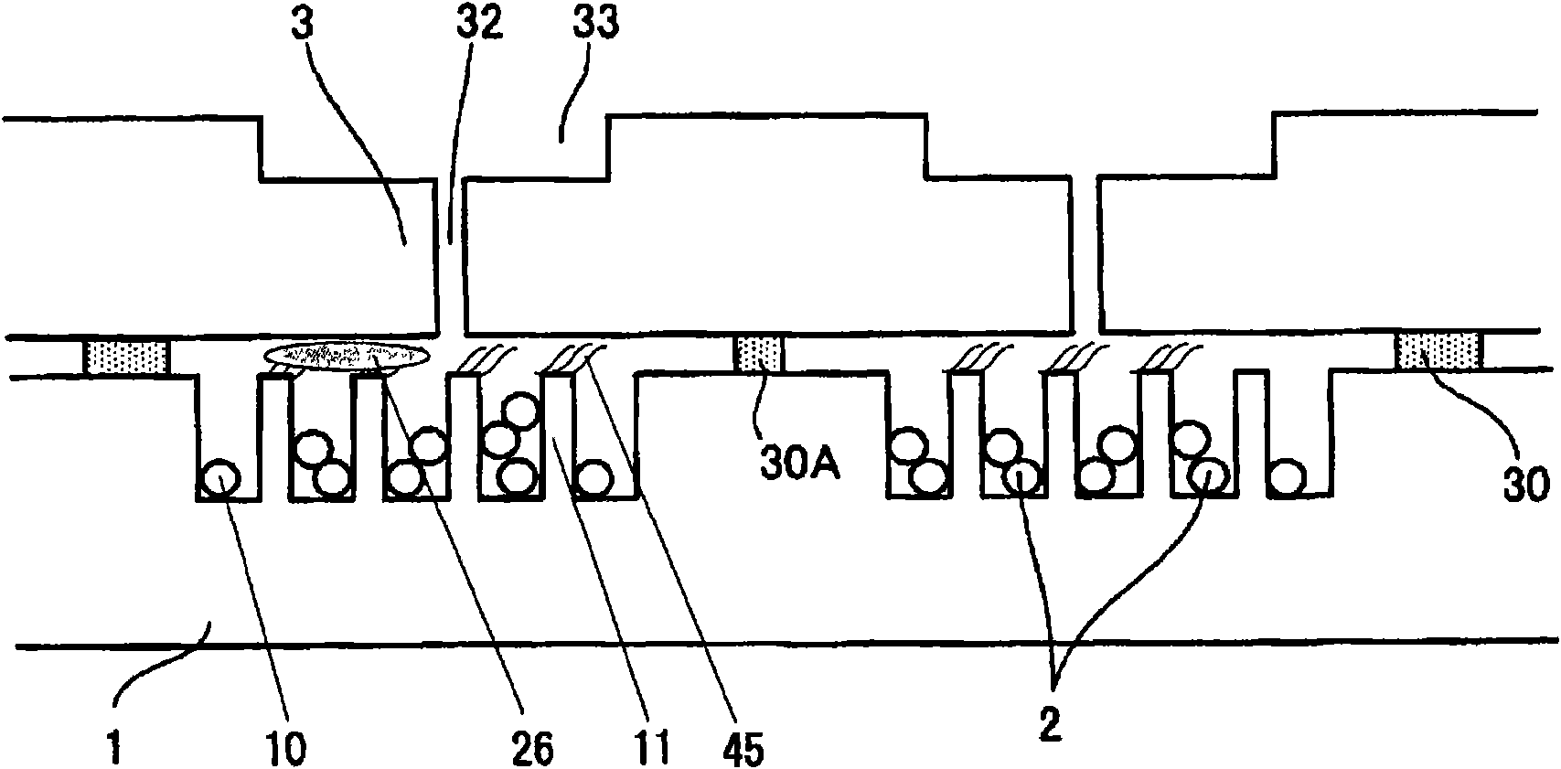
[0011] However, when a liquid containing a test substance is applied to an analysis chip that uses microparticles for stirring as described above, bubbles may remain on the surface of the analysis chip substrate or on the surface of the microparticles, or bubbles may be generated in the reaction solution.
The generated air bubbles become obstacles, and there is a problem that the reaction between the selective binding substance and the test substance is hindered in the part where the air bubbles remain
In addition, since there is a difference in reaction between the portion where the air bubbles remain and other portions, there is a problem that a difference in detection sensitivity occurs or a decrease in detection sensitivity occurs on the analysis chip.
[0012] In addition, when accommodating or injecting stirring particles into the gap between the analysis chip substrate and the cover, static electricity may be generated, making it difficult to inject the particles into the gap, or it may not be possible to inject a sufficient amount of particles.
In addition, the injected particles may aggregate and become immobile. In this state, when the test substance solution is injected into the space surrounded by the cover and the substrate, there may be air bubbles mixed in due to the inability of the solution to diffuse to the site where the particles aggregate, The question of response differences

Method used


Image

  • Analysis chip and analysis method
  • Analysis chip and analysis method
  • Analysis chip and analysis method

Examples


Embodiment 1

[0142] (1) Fabrication of substrates for analytical chips

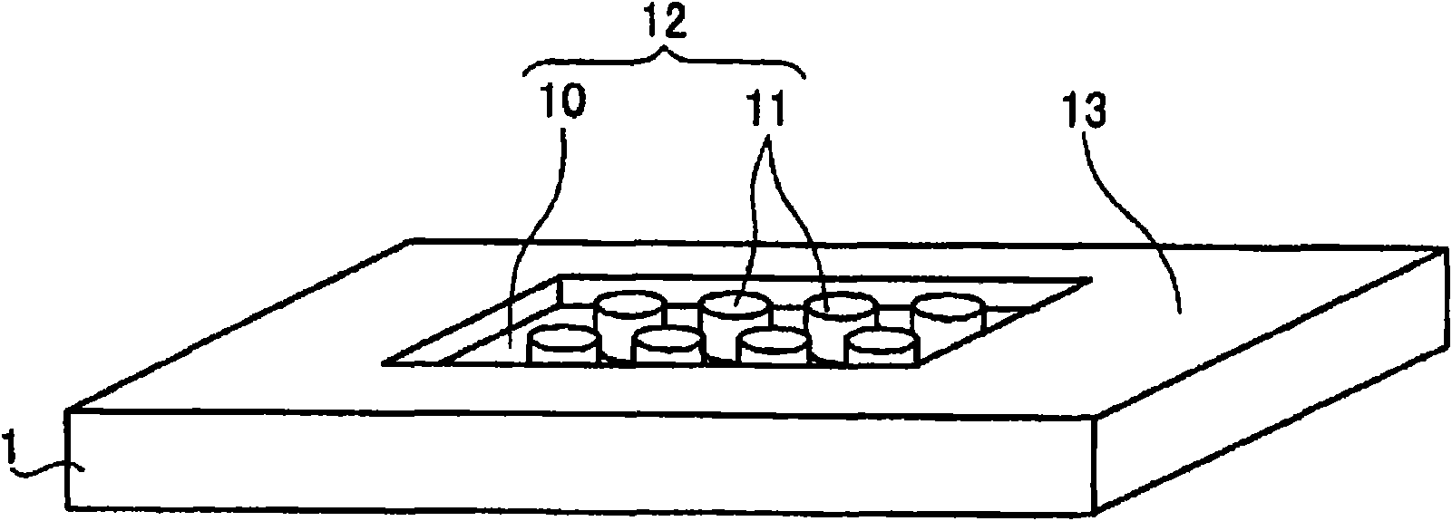
[0143] Using LIGA (Lithographie Galvanoformung Abformung) technique which is a well-known method, a mold for injection molding was produced, and a substrate made of polymethyl methacrylate (PMMA) having the following shape was obtained by injection molding. The average molecular weight of the PMMA used was 50,000, carbon black (#3050B manufactured by Mitsubishi Chemical) was contained in PMMA at a ratio of 1% by weight, and the substrate was made black. The spectral reflectance and spectral transmittance of the black substrate were measured. As a result, the spectral reflectance was 5% or less at any wavelength in the visible light region (wavelength of 400nm to 800nm). The rate is 0.5% or less. Neither the spectral reflectance nor the spectral transmittance has a specific spectral pattern (peak, etc.) in the visible light region, and the spectrum is similarly flat. It should be noted that the spectral reflectance i...

Embodiment 2

[0167] Evaluation using the analysis chip 1 was performed in the same manner as in Example 1, except that the test substance solution prepared in Example 1 (6) was degassed as described below.

[0168] 175 μl of the test substance solution was put into a 0.2 ml PCR tube (72.737.002 manufactured by Ashisuto Co., Ltd.), and degassed in a degasser (aspirator NDA-015 manufactured by ULVAC Co., Ltd.) with the cap opened. The ultimate pressure during degassing is 50hPa in the display of the device, and the degassing time is 25 minutes.

[0169] In the same manner as in Example 1 (7), the number of bubbles in the test substance solution observed on the substrate after the hybridization reaction was counted, and the average value of the number of bubbles per 1 time obtained after implementing the result 6 times was: 0.4 (Table 1).

[0170] In addition, in the same manner as in Example 1 (8), when the difference in background signal value (CV value) was calculated, it was 6.7% (Table ...

Embodiment 3

[0181] In Example 1 (4), sodium deoxycholate (one type of anionic surfactant) was used instead of sodium dodecyl sulfate (SDS) as a surfactant, and 120 mg of the surfactant-coated The treated microparticles were prepared to produce "Analysis Chip 3". Using this analysis chip 3, the test substance solution was degassed and evaluated in the same manner as in Example 2.

[0182] The operability of microparticle injection was evaluated in the same manner as in Example 1 (5). As a result, the average time required after 10 implementations was 3 minutes to 5 minutes, so the operability evaluation of microparticle encapsulation into the analysis chip 3 was " B" (Table 2).

[0183] In this analysis chip 3, the number of bubbles generated in the test substance solution was counted after the hybridization reaction in the same manner as in Example 1 (7). As a result, the average number of bubbles after 10 implementations was 0.6 (Table 2).

[0184] In addition, the difference in backgr...


PUM

PropertyMeasurementUnit
surface roughnessaaaaaaaaaa
diameteraaaaaaaaaa
surface roughnessaaaaaaaaaa

Abstract

This invention is directed to an analysis chip comprising a substrate having a surface on which a selective binding substance is immobilized; a cover member adhered to the substrate; and particles movably contained or injected in a void between the substrate and the cover member; wherein the surfaces of the particles are coated with a surfactant. By this invention, generation of bubbles which inhibit the selective reaction between the test substance and the immobilized selective binding substance is suppressed, thereby reducing the deviation of data, suppressing the lowering of sensitivity, and promoting the reproducibility of the measurement.

Description

technical field [0001] The present invention relates to an analysis chip having a substrate immobilized with a selectively binding substance, that is, a substance that selectively binds to a test substance, and a method for analyzing a test substance using the analysis chip. Background technique [0002] The analysis chip has a substrate immobilized with selective binding substances such as genes, proteins, lipids, sugars, etc., and reacts the selective binding substance test substance on the substrate as a normal solution to analyze the test substance based on the reaction result Existence, state of existence, quantity, etc. As the substrate, generally, glass, metal, or resin substrates can be used. [0003] As one of the proposals for an analysis chip, there is an analysis chip in which molecules such as DNA are arranged at a high density on a substrate in order to simultaneously measure the expression of several hundreds to tens of thousands of genes, which is sometimes ...

Claims


Application Information

Patent Timeline
Patent Type & Authority Applications(China)
IPC IPC(8): G01N33/53C12M1/00C12N15/09C12Q1/68G01N33/543G01N37/00
CPCB01J2219/00722G01N33/54393B01F13/0052B01J2219/00387B01J2219/0061B01J2219/00621B01J2219/00659B01J2219/00479B01J2219/00317B01J2219/00596B01J2219/00509B01J2219/00626B01J19/0046B01F13/0059C12Q1/6837B01J2219/00608B01F33/251B01F33/30C12Q2527/125C12Q2563/155C12Q1/6834
Inventor 野村修黑田俊彦信正均村尾康雄
Owner TORAY IND INC
Learn More