Compound conducting film and touch screen using same

A composite conductive film and touch screen technology, which is applied in the direction of electrical digital data processing, input/output process of data processing, optics, etc., can solve the problems of reducing the strength of the film, increasing the light absorption of the material, and the conductivity and uniformity of the film layer. , to achieve the effect of improving light transmission performance, satisfying input durability, improving performance and uniformity

Inactive Publication Date: 2009-11-18
甘国工
View PDF3 Cites 30 Cited by
  • Summary
  • Abstract
  • Description
  • Claims
  • Application Information

AI Technical Summary

Problems solved by technology

It is known that the larger the size of the conductive crystal grains, the more uniform the grain size distribution, and the better and more stable the overall conductivity of the film. Therefore, the conductivity and uniformity of the coating layer are not as good as those of the magnetron sputtering layer. If

Method used


Image

  • Compound conducting film and touch screen using same
  • Compound conducting film and touch screen using same
  • Compound conducting film and touch screen using same

Examples


Embodiment 1

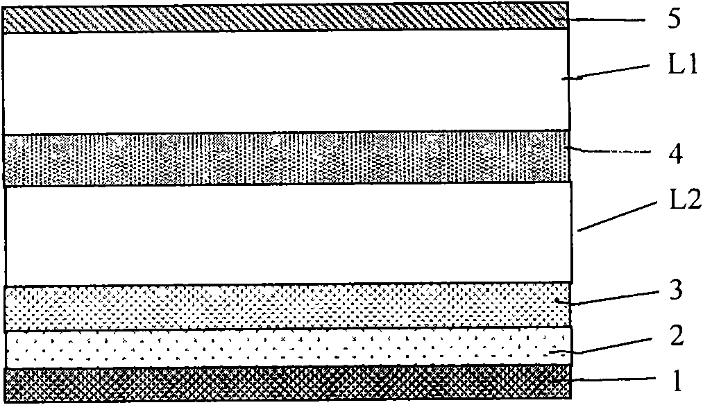
[0029] figure 1 The structure diagram of the composite conductive film of the present embodiment 1 is given, see figure 1 , the first flexible light-transmitting base layer L1 with the upper and lower surfaces is a PET film of 125 μm, and the second flexible light-transmitting base layer L2 with the upper and lower surfaces is a PET film of 75 μm, located on the lower surface of the first flexible light-transmitting base layer L1 and The elastic adhesive layer 4 between the upper surfaces of the second flexible light-transmitting base layer L2 can be made of hot-melt glue or resin, with a thickness of 15 μm. The inorganic dielectric film system and transparent conductive film layer formed by high refractive index inorganic dielectric film and low refractive index inorganic dielectric film are deposited by vacuum magnetron sputtering to form an overall transmittance of more than 80% in the light wavelength range of 380nm to 780nm Optical interference film system. A layer of h...

Embodiment 2

[0047] Figure 4 The structural diagram of the composite conductive film in Example 2 is given. see Figure 4 , this embodiment is basically the same as Embodiment 1, and the difference from Embodiment 1 is that the film system can be formed by interlacing the multi-layer inorganic dielectric film 3 with high refractive index and the inorganic dielectric film 2 with low refractive index, and can also achieve a very high High transmittance. The advantage of the multi-layer film system is that it can reduce the degree of interference of the coating on the color of the transmitted light.

Embodiment 3

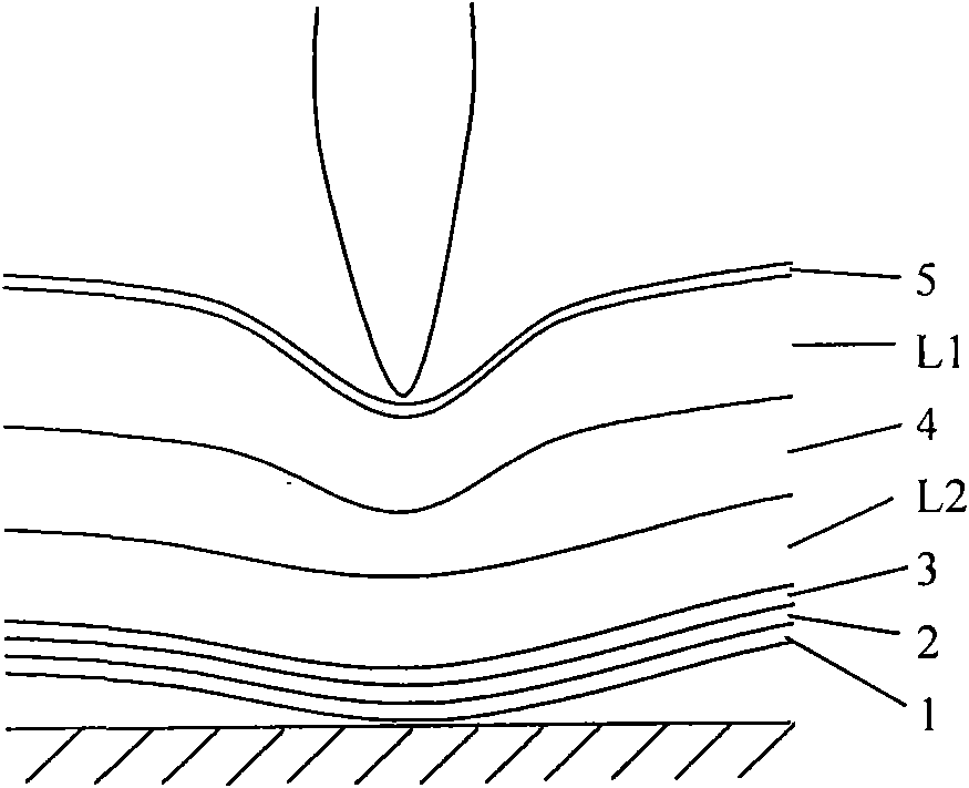
[0049] Figure 5 A schematic diagram of the structure of the touch screen film group in Example 3 is given. see Figure 5 According to the composite conductive film of the present invention, as the upper substrate P1 of the touch screen module, it is opposed to another lower substrate P2 separated by spacers and spacers 6, and the lower substrate P2 can be conductive glass, other conductive films Or the composite conductive film of the present invention. The edge of the transparent conductive film layer is plated / printed with electrodes, which are led out by wires. The composite conductive film according to the present invention can also be used as the lower substrate P2 of the touch screen module.


PUM

PropertyMeasurementUnit
Thicknessaaaaaaaaaa
Thicknessaaaaaaaaaa
Thicknessaaaaaaaaaa

Abstract

The invention discloses a compound conducting film which comprises a first flexible transmitting base layer L1 with an upper surface and a lower surface, a second flexible transmitting base layer L2 with an upper surface and a lower surface, an elastic adhesive layer positioned between the first flexible transmitting base layer L1 and the second flexible transmitting base layer L2, inorganic dielectric film systems of at least two layers of dielectric films formed by sequentially staggering high-index inorganic dielectric films and low-index inorganic dielectric films and settled in sequence on the lower surface of the second flexible transmitting base layer L2 , and a transparent conducting film layer positioned at the outermost layer of the film system, wherein the thickness of the transparent conducting film layer meets the value being 3-10mm required by a square resistance, at least two dielectric film systems consisting of the high-index inorganic dielectric and both the low-index inorganic dielectric are settled by adopting a vacuum magnetron sputtering method so that optical interference film systems with whole transmittance rate reaching more than 80 percent is formed. The invention also provides a touch screen using the compound conducting film.

Description

Technical field: [0001] The invention relates to a composite conductive film with high transmittance and high durability, and various touch screens using the film. Background technique: [0002] Conventional conductive films for touch screens are usually formed by sputtering or coating a conductive layer directly on a flexible substrate. The transmittance of the conductive film in this way is not high, so the picture placed under the touch screen is usually dark. After multiple touches by the user, the conductive layer is easily broken and causes a change in the resistance value, resulting in a shift in the position calculated by the electric shock or unresponsive operation. [0003] For example, the application number is 02803118.0, and the patent application titled transparent conductive laminated body and transparent touch panel using the laminated body discloses a conductive laminated film with high light transmittance. On at least one surface of the organic polymer fil...

Claims


Application Information

Patent Timeline
IPC IPC(8): G02B1/11B32B7/02B32B7/12B32B33/00B32B9/00G06F3/041G02B1/111G02B1/116
Inventor 甘国工
Owner 甘国工
Why Eureka
Try Eureka