Structure and manufacturing method of packaged base plate

A technology for packaging substrates and substrates, which is applied in semiconductor/solid-state device manufacturing, electrical components, electrical solid-state devices, etc., and can solve problems such as limiting the spacing of metal bumps 15

Inactive Publication Date: 2009-11-25
PHOENIX PRECISION TECH CORP
View PDF0 Cites 1 Cited by
  • Summary
  • Abstract
  • Description
  • Claims
  • Application Information

AI Technical Summary

Problems solved by technology

[0007] The above drawings illustrate that in the prior art, under a certain pad pitch, due to the limitation of the size of the electrical connection pads 12a, only one circuit 12b can be arranged in the space between adjacent electrical connection pad

Method used


Image

  • Structure and manufacturing method of packaged base plate
  • Structure and manufacturing method of packaged base plate
  • Structure and manufacturing method of packaged base plate

Examples


Embodiment 1

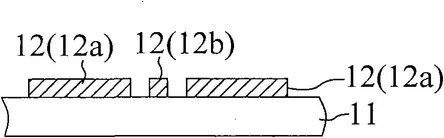
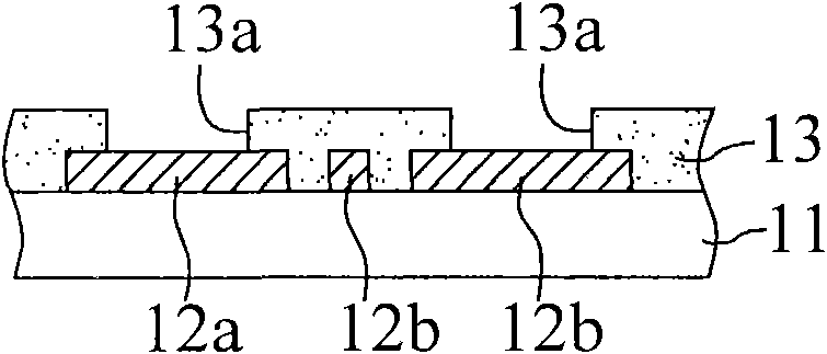
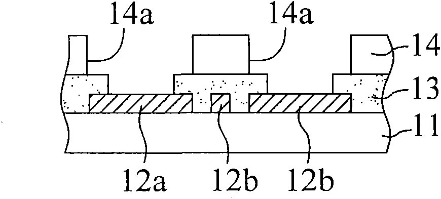
[0041] Figure 4A to Figure 4D It is a schematic cross-sectional view of the manufacturing method of the packaging substrate structure of a preferred embodiment of the present invention, Figure 5A to Figure 5D Its corresponding top view diagram. First, see Figure 4A A packaging substrate 41 is provided, and a patterned metal layer is formed on the surface of the packaging substrate 41 as the circuit layer 42 . In this embodiment, the patterned metal layer is a structure formed by stacking a seed layer and a metal layer on the seed layer. The material of the seed layer and the metal layer used in this embodiment is copper.

[0042] see Figure 4A and Figure 5A The circuit layer 42 includes a plurality of electrical connection pads 42a and circuits 42b. The planar shape of the electrical connection pads 42a is a prolate rectangle, so as to improve the flexibility of circuit layout space.

[0043] Compared with existing packaging substrate structures (see Figure 2A ), th...

Embodiment 2

[0049] Except that the plane shapes of the electrical connection pads and the openings of the solder resist layer are elliptical, the structure and manufacturing method of the packaging substrate of this embodiment are the same as those of the first embodiment. So I won't repeat them here.

[0050] Compared to Example 1 Figure 4B and Figure 5B , Figure 7 It is a three-dimensional schematic view of the packaging substrate structure of this embodiment, including: a substrate body 41 , an electrical connection pad 42 a , a circuit 42 b , a solder resist layer 43 and a solder resist layer opening 43 a. Figure 8 for Figure 7 In the top view of , the plane shapes of the electrical connection pad 42a (indicated by a dotted line) and the solder mask opening 43a are both elliptical.

[0051] Similarly, since the planar shape of the electrical connection pad and the opening of the solder mask layer is flat and long, the flexibility of the circuit layout space can be improved, t...


PUM


Abstract

The invention relates to a structure and a manufacturing method of a packaged base plate. The packaged base plate comprises a base plate body, a welding preventing layer and metal projections, wherein the base plate body is provided with a circuit layer on the surface, the circuit layer is provided with a plurality of electrically connected pads of which the planes are prolate so as to improve the flexibility of circuit distribution space; the welding preventing layer covers the base plate body and is provided with a plurality of open pores corresponding to the electrically connected pads, wherein the plane shapes of the open pores of the welding preventing layer are prolate; and the metal projections are matched with the open pores in the welding preventing layer and correspond to the electrically connected pads. When used for manufacturing the packaged base plate of a multilayer plate, the invention can reduce the layers of a circuit layer increasing structure of the multilayer plate because the distributed circuits can be increased in the space between two adjacent electrically connected pads, thereby lowering the manufacturing cost.

Description

technical field [0001] The present invention relates to a package substrate structure and its manufacturing method, in particular to a package substrate structure and its manufacturing method which can increase the number of circuits between adjacent electrical connection pads or reduce the pitch of bumps. Background technique [0002] At present, in most semiconductor packaging structures, the back surface of the semiconductor chip is pasted on the surface of the substrate body on the side where the chip is placed, and then wire bonding is performed, or the active surface of the semiconductor chip is bonded to the substrate by flip-chip bonding (Flip chip). The crystal side surface of the body is electrically connected, and then solder balls are planted on the ball side surface of the substrate body to electrically connect to external electronic devices such as printed circuit boards. [0003] Figure 1A to Figure 1D It is a schematic cross-sectional view of the manufacturi...

Claims


Application Information

Patent Timeline
IPC IPC(8): H01L23/488H01L23/498H01L21/48
CPCH01L2924/0002
Inventor 胡文宏
Owner PHOENIX PRECISION TECH CORP
Why Eureka
Try Eureka