Semiconductor element isolating structure and forming method thereof

A technology of component isolation and isolation structure, which is applied in the direction of semiconductor devices, semiconductor/solid-state device manufacturing, semiconductor/solid-state device components, etc., can solve problems such as short circuit and integrated circuit failure, and achieve the effect of preventing bridging

Active Publication Date: 2009-12-09
UNITED MICROELECTRONICS CORP
View PDF0 Cites 8 Cited by
  • Summary
  • Abstract
  • Description
  • Claims
  • Application Information

AI Technical Summary

Problems solved by technology

Since the etch stop layer of the contact window on the shallow trench isolation structure has gaps or holes, and when the chemical vapor deposition of tungsten is performed, the tungsten metal has a strong ability to fill holes, so in the process of forming the tungsten contact plug, Tungsten metal will also fill the gap or hole in the etch stop layer of the contact window, so that two adjacent tungsten contact plugs will bridge and short each other, causing the integrated circuit to fail to operate normally

Method used


Image

  • Semiconductor element isolating structure and forming method thereof
  • Semiconductor element isolating structure and forming method thereof
  • Semiconductor element isolating structure and forming method thereof

Examples


Embodiment Construction

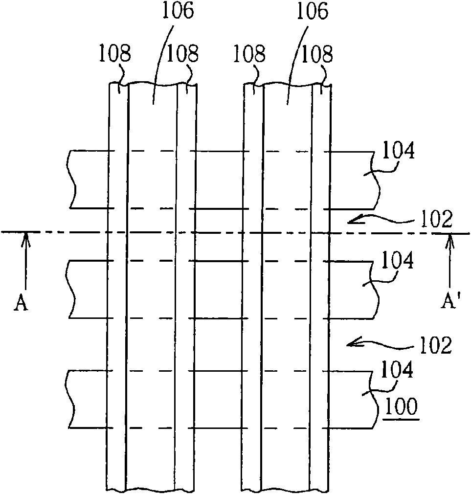
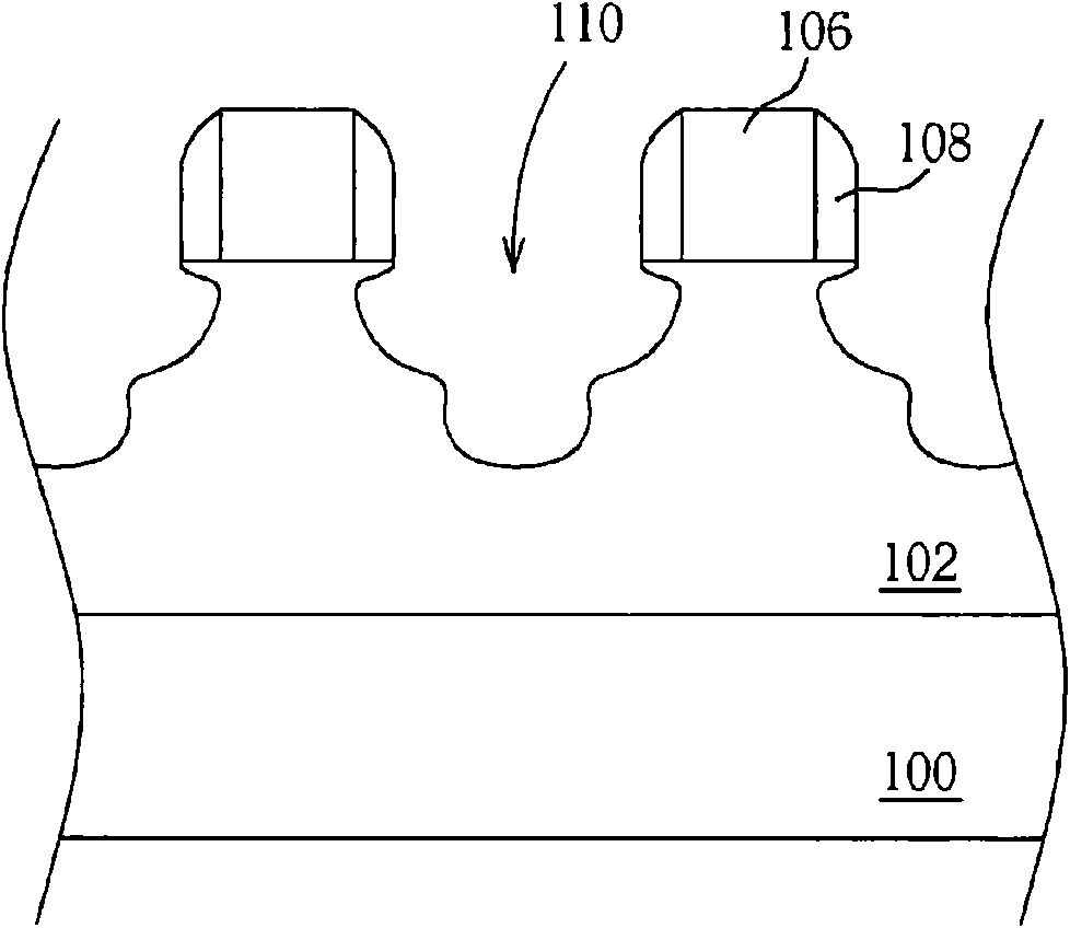
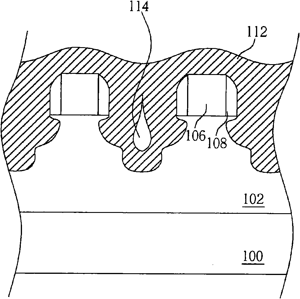
[0027] Please refer to Figure 4 to Figure 9 , Figure 4 It is a semiconductor element of a preferred embodiment of the present invention, such as a dynamic random access memory (DRAM) storage unit (memory cell), a schematic top view of the layout, Figure 5 to Figure 9 For a preferred embodiment of the present invention along Figure 4 Schematic diagram of the formation method of the semiconductor element isolation structure of the BB' line. Such as Figure 4 and Figure 5 As shown, first, a substrate 200 is provided, such as a silicon wafer or a silicon-on-insulator substrate. The substrate 200 includes at least one shallow trench isolation structure 202 and a plurality of gate structures 204 disposed on the shallow trench isolation structure 202 and the substrate 200, wherein the shallow trench isolation structure 202 defines a plurality of active regions 206, and The shallow trench isolation structure 202 is used to isolate each active region 206 . In addition, space...


PUM


Abstract

The invention discloses a semiconductor element isolating structure and a forming method thereof. The forming method of the semiconductor element isolating structure comprises the following steps: firstly, providing a substrate with at least one shallow-groove isolating structure; then, carrying out a metal silicification process to form a dent on the surface of the shallow-groove isolating structure; forming a covering layer to cover the substrate and fill the dent; etching the covering layer to remove the covering layer outside the dent; and finally, forming a contact window etching-stopping layer to cover the substrate and fill the dent. The covering layer is filled in the dent in advance so that the contact window etching-stopping layer covered on the substrate and filled in the dent can not generate gaps or holes.

Description

technical field [0001] The invention relates to a semiconductor element isolation structure, especially a method for forming the semiconductor element isolation structure, which is used to avoid gaps in the etching stop layer of the contact window, thereby preventing short circuit of the subsequently formed contact plug. Background technique [0002] The field oxide (FOX) structure traditionally used to isolate semiconductor elements is formed by the local oxidation of silicon (LOCOS), but the isolation structure formed by the isolation technology using the local oxidation of silicon has a field The horizontal growth of the oxide layer, the horizontal diffusion of field dopant ions, the thinning effect of the small-sized field oxide layer, and the erosion of the bird's beak, etc., have developed a shallow trench isolation structure (shallow trench isolation structure, STI structure), To apply to the manufacture of deep submicron integrated circuits. The shallow trench isola...

Claims


Application Information

Patent Timeline
Patent Type & Authority Applications(China)
IPC IPC(8): H01L21/768H01L21/762H01L27/02H01L23/522
CPCH01L2924/0002
Inventor 吕水烟叶洸玮陈信琦陈琮文朱庆芳白启宏陈界得
Owner UNITED MICROELECTRONICS CORP
Why Eureka
Try Eureka