Simultaneous detection biological sensor by utilizing capacitance and conduction of quasi-one-dimensional nanometer material field effective tube
A biosensor and nanomaterial technology, which is applied in the field of quasi-one-dimensional nanomaterial field effect tube capacitance and conductance simultaneous detection of biosensors, can solve problems such as viscous damping and sensitivity decline, achieve high sensitivity, simple processing technology, and easy popularization and application. Effect
- Summary
- Abstract
- Description
- Claims
- Application Information
AI Technical Summary
Problems solved by technology
Method used
Image
Examples
Embodiment 1
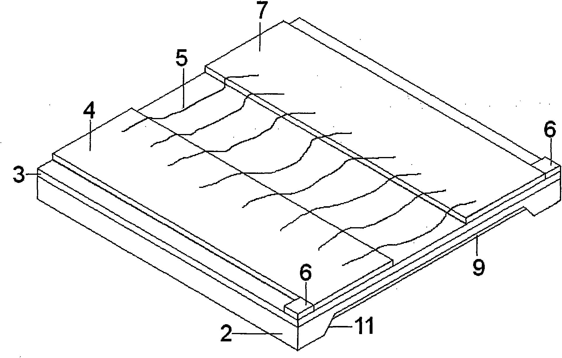
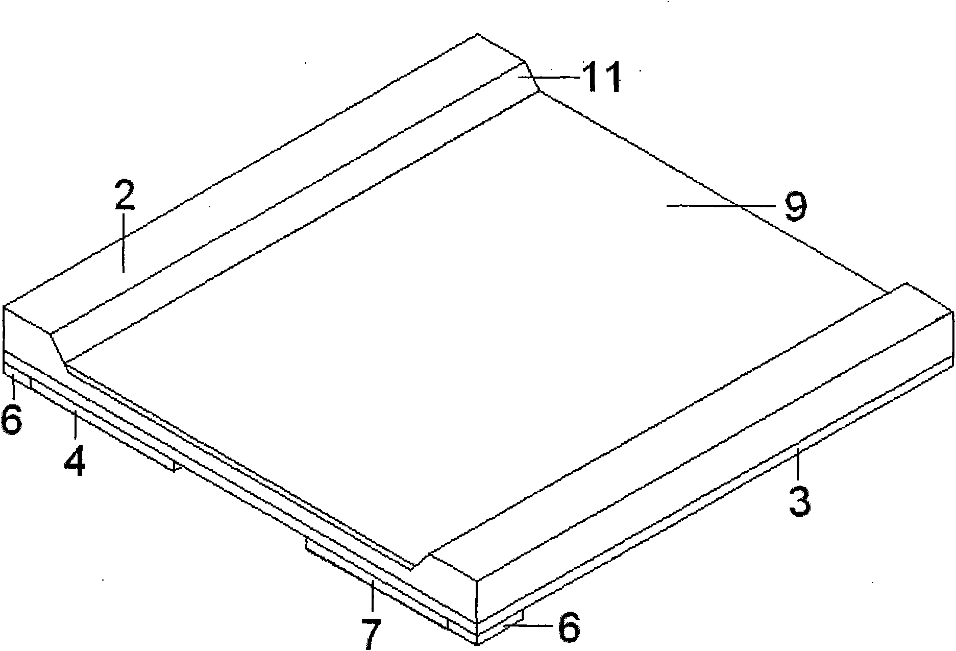
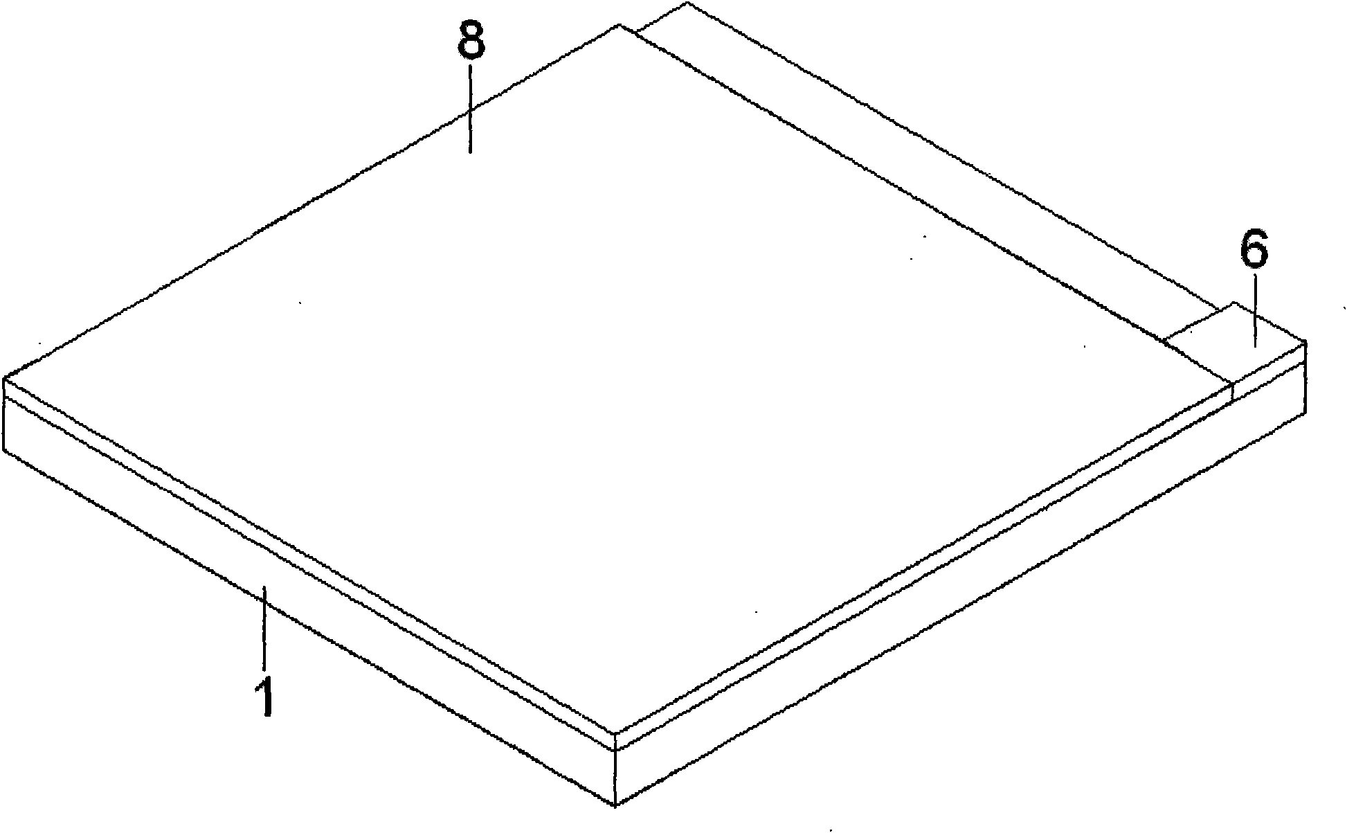
[0019] like figure 1 Shown is a schematic diagram of a three-dimensional structure of a quasi-one-dimensional nanomaterial field effect tube for simultaneously detecting the upper surface of a silicon wafer on a biosensor, as shown in figure 2 Shown is a schematic diagram of a three-dimensional structure of a quasi-one-dimensional nanomaterial field effect tube for simultaneously detecting the lower surface of a silicon wafer on a biosensor, as shown in image 3 Shown is a schematic diagram of the three-dimensional structure of the silicon chip under the biosensor for simultaneous detection of the capacitance and conductance of the quasi-one-dimensional nanomaterial field effect tube.
[0020] like Figure 4 As shown, the quasi-one-dimensional nanomaterial field effect tube capacitance conductance simultaneous detection biosensor includes two parts, the lower silicon wafer 1 and the upper silicon wafer 2, which are mainly composed of an insulating layer 3, a metal electrode ...
Embodiment 2
[0040] like Figure 5 Shown is a schematic diagram of a three-dimensional structure of a quasi-one-dimensional nanomaterial field effect tube for simultaneously detecting the upper surface of a silicon wafer on a biosensor, as shown in figure 2 Shown is a schematic diagram of a three-dimensional structure of a quasi-one-dimensional nanomaterial field effect tube for simultaneously detecting the lower surface of a silicon wafer on a biosensor, as shown in image 3 Shown is a schematic diagram of the three-dimensional structure of the silicon chip under the biosensor for simultaneous detection of the capacitance and conductance of the quasi-one-dimensional nanomaterial field effect tube.
[0041] like Image 6 As shown, the quasi-one-dimensional nanomaterial field effect tube capacitance and conductance simultaneous detection biosensor includes two parts, a lower silicon wafer 1 and an upper silicon wafer 2, which are mainly composed of an insulating layer 3, a metal interdigi...
PUM
 Abstract
Description
Claims
Application Information


