Ultrathin pre-plating layer lead frame and preparation method thereof
A lead frame and pre-coating technology, which is applied in the field of ultra-thin pre-coated lead frame structure and its preparation process, can solve problems such as embrittlement of solder joints, hidden reliability concerns, easy breakage, etc., and achieve reduced thickness and low diffusion rate , increase the effect of antioxidant
- Summary
- Abstract
- Description
- Claims
- Application Information
AI Technical Summary
Problems solved by technology
Method used
Image
Examples
Embodiment 1
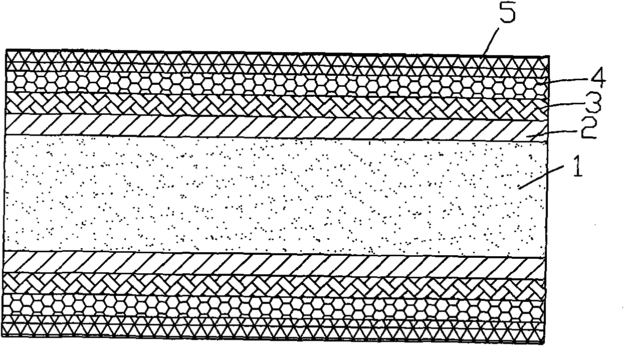
[0039] Such as figure 1 The ultra-thin pre-plated lead frame shown is the first embodiment of the present invention. It includes a copper alloy lead frame base 1 on which a tin (Sn) metal layer 2, a nickel (Ni) metal layer 3, and a palladium ( Pd) metal layer 4 and gold (Au) metal layer 5.
[0040] In this embodiment, the thickness of the Sn metal layer is 3 nm, the thickness of the Ni metal layer is 250 nm, the thickness of the nano-level Pd metal layer is 10 nm, and the thickness of the nano-level Au metal layer is 2 nm.
[0041] In practical applications, the thickness of the Sn metal layer can be arbitrarily selected in the range of 1-10nm, the thickness of the Ni metal layer can be selected in the range of 50-350nm; the thickness of the Pd metal layer can be appropriately selected in the range of 5-15nm Selection; the thickness of the Au metal layer can be appropriately selected in the range of 1-10 nm.
Embodiment 2
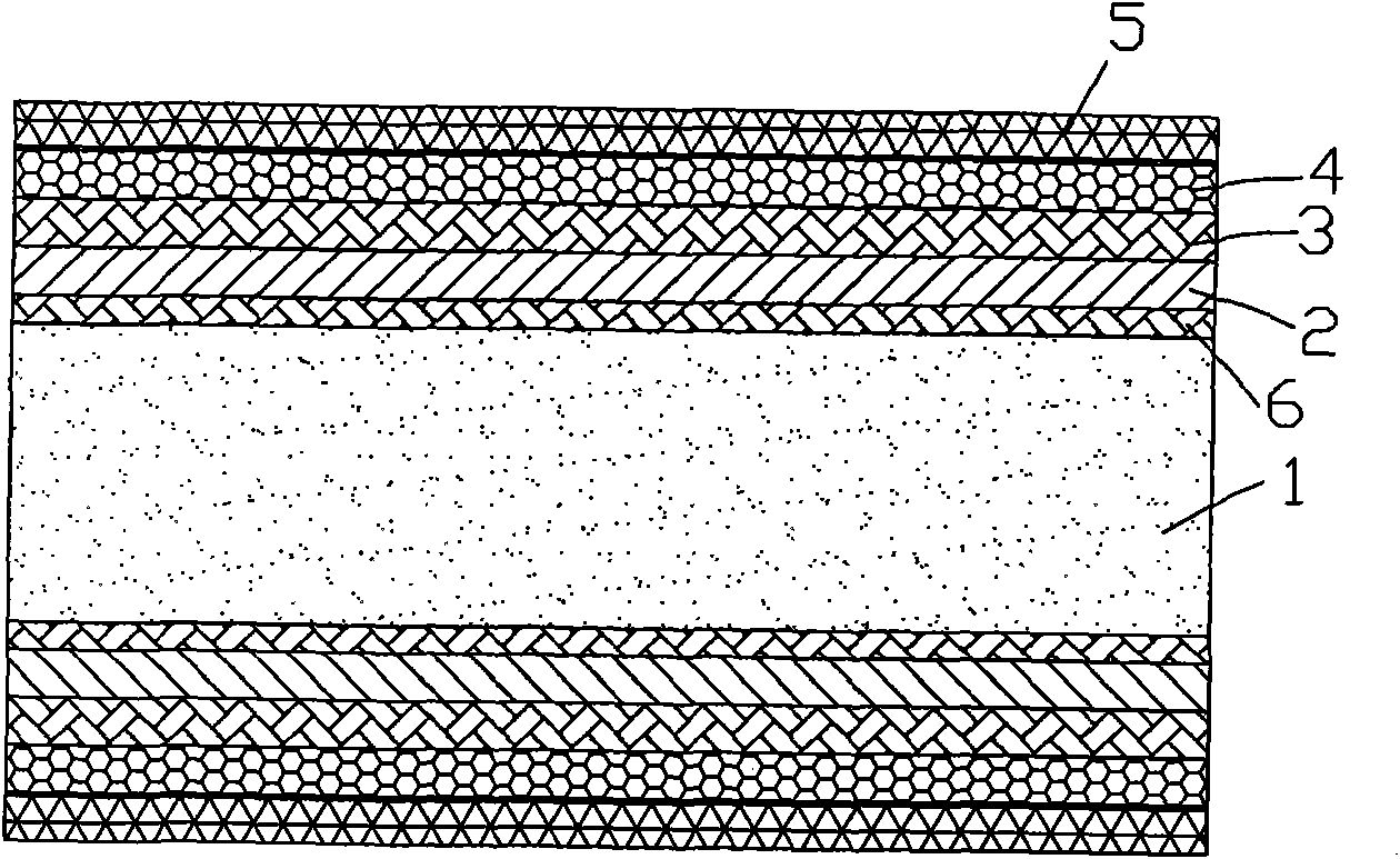
[0043] Such as figure 2 The ultra-thin pre-plated lead frame shown is the second embodiment of the present invention. It includes a copper alloy lead frame substrate 1 on which a first nickel (Ni) metal layer 6, a tin (Sn) metal layer 2, A second nickel (Ni) metal layer 3, a palladium (Pd) metal layer 4, and a gold (Au) metal layer 5.
[0044] In this embodiment, the thickness of the first Ni metal layer 6 is 50 nm, the thickness of the Sn metal layer is 3 nm, the thickness of the second Ni metal layer 3 is 200 nm, the thickness of the Pd metal layer is 10 nm, and the thickness of the Au metal layer is 2 nm. .
[0045] In practical applications, the thickness of the first Ni metal layer 6 can be arbitrarily selected in the range of 0 to 200 nm, and the thickness of the second Ni metal layer can be selected in the range of 50 to 350 nm; the thickness of the Sn metal layer can be 1 It is arbitrarily selected within the range of ~10nm, the thickness of the Pd metal layer can be appr...
Embodiment 3
[0047] Example 3 of the present invention is a method for preparing lead frames by high-frequency pulse electrodeposition. Preparation of the pre-plated layer structure described in Examples 1 and 2, specifically includes:
[0048] 1) Activate the copper alloy lead frame matrix: first immerse the lead frame in 8%-20% sulfuric acid solution for 10-30s, then rinse with deionized water; then immerse the lead frame in 8%-20% Soak in hydrochloric acid solution for 10-30s, then rinse with deionized water and blow dry for electrodeposition treatment.
[0049] 2) Sn metal layer electroplating solution and electroplating process: The working frequency of the high-frequency pulsed electricity used is 200Hz-500Hz, and the current density is 0.1-2A / dm 2 , The duty cycle used is 30%-60%; the plating solution used is 10-40g / L stannous methanesulfonate, 20-40g / L stannous sulfate, 30-50g / L cresol sulfonic acid, sulfuric acid 10~20g / L, 4-4'tetramethyldiaminodiphenylmethane 0.1~0.8g / L, gelatin 0.05~...
PUM
| Property | Measurement | Unit |
|---|---|---|
| thickness | aaaaa | aaaaa |
| current density | aaaaa | aaaaa |
| thickness | aaaaa | aaaaa |
Abstract
Description
Claims
Application Information
 - R&D
- Intellectual Property
- Life Sciences
- Materials
- Tech Scout
- Unparalleled Data Quality
- Higher Quality Content
- 60% Fewer Hallucinations
Browse by: Latest US Patents, China's latest patents, Technical Efficacy Thesaurus, Application Domain, Technology Topic, Popular Technical Reports.
© 2025 PatSnap. All rights reserved.Legal|Privacy policy|Modern Slavery Act Transparency Statement|Sitemap|About US| Contact US: help@patsnap.com


