(GeTe)*(SbTe*)*base dilute magnetic semiconductor material for storing information

A dilute magnetic semiconductor and information storage technology, applied in the field of microelectronics, can solve problems such as doping

Inactive Publication Date: 2010-01-20
BEIJING UNIV OF TECH
View PDF0 Cites 14 Cited by
  • Summary
  • Abstract
  • Description
  • Claims
  • Application Information

AI Technical Summary

Problems solved by technology

However, the method of doping magnetic elements in the Ge-Sb-Te phase change material and using the difference in magnetic

Method used


Image

  • (GeTe)*(SbTe*)*base dilute magnetic semiconductor material for storing information
  • (GeTe)*(SbTe*)*base dilute magnetic semiconductor material for storing information
  • (GeTe)*(SbTe*)*base dilute magnetic semiconductor material for storing information

Examples


Embodiment 1

[0016] Using double target co-sputtering method with Mn and Ge 2 Sb 2 Te 5 Mn-Ge prepared on Si wafer by two relatively independent targets 2 Sb 2 Te 5 Phase-change thin film material, meanwhile, in order to observe the microstructure of the phase-change memory material in the present invention, the method of dual-target co-sputtering is also used to use Mn and Ge 2 Sb 2 Te 5 Two relatively independent targets prepared Mn-Ge on the TEM grid 2 Sb 2 Te 5 Phase change film materials. Argon gas pressure during sputtering is 0.5Pa, Mn and Ge 2 Sb 2 Te 5 The power on the target is 60 watts of direct current and 100 watts of radio frequency respectively, and the thickness of the prepared phase change thin film material can be controlled by controlling the sputtering time. X-ray fluorescence spectrum analysis showed that the composition of the material was Mn 0.35 (Ge 2 Sb 2 Te 5 ) 0.65 .

[0017] Will get Mn 0.35 (Ge 2 Sb 2 Te 5 ) 0.65 The phase-change thin fi...

Embodiment 2

[0021] co-sputtering with Co and Ge 2 Sb 2 Te 5 Co-Ge prepared on silicon substrate by two relatively independent targets 2 Sb 2 Te 5 Phase change film materials. Argon gas pressure during sputtering is 0.5Pa, Co and Ge 2 Sb 2 Te 5 The power on the target is 200 watts of radio frequency and 100 watts of radio frequency respectively, and the thickness of the prepared phase change thin film material can be controlled by controlling the sputtering time. X-ray fluorescence spectroscopic analysis showed that the composition of the material was Co 0.04 (Ge 2 Sb 2 Te 5 ) 0.96 .

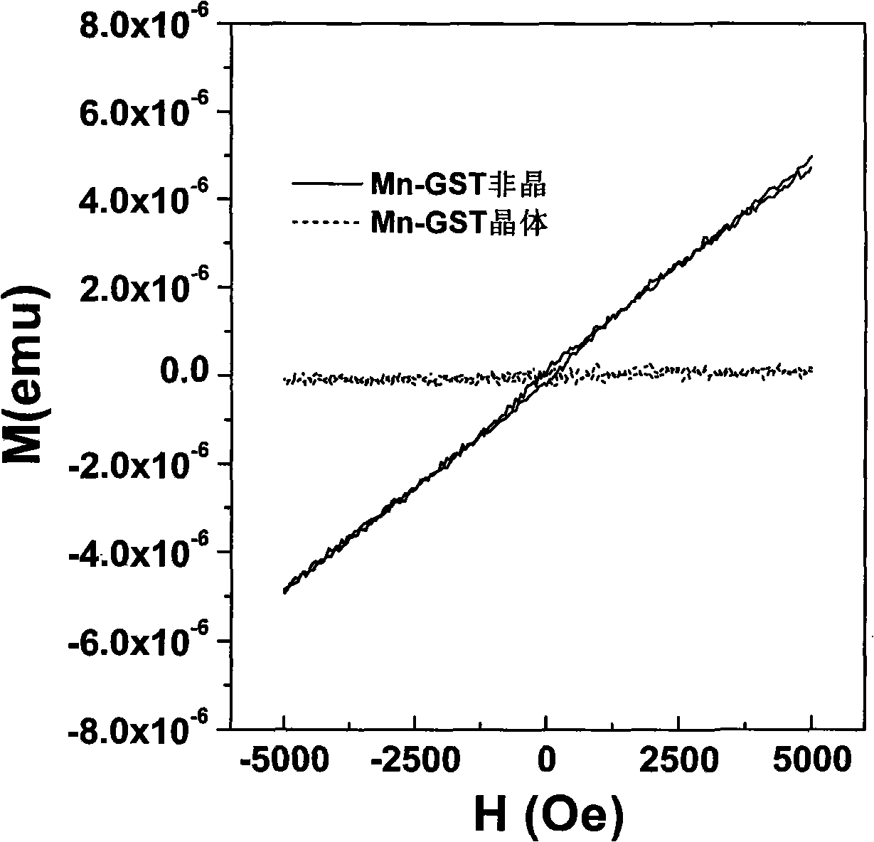
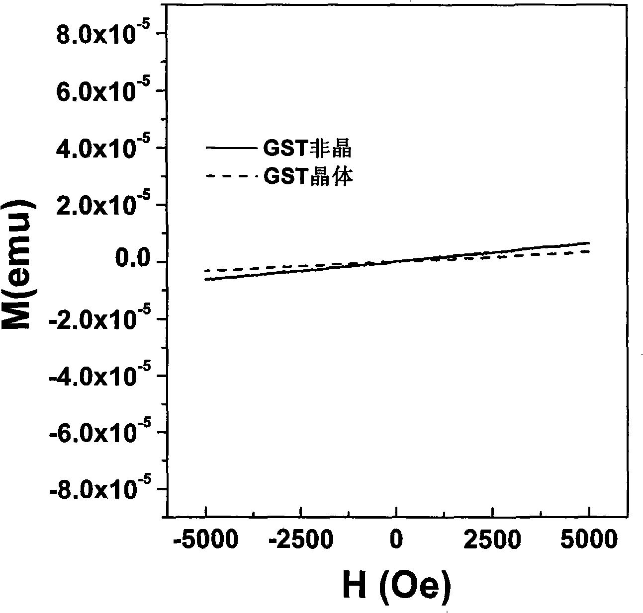
[0022] Will get Co 0.04 (Ge 2 Sb 2 Te 5 ) 0.96 The phase-change thin film material is annealed at a temperature of 300 degrees under the protection of a high-purity argon atmosphere. Figure 4 Shown are the hysteresis loops of the samples measured with an AC gradient magnetometer before and after annealing treatment and the enlarged local hysteresis loops (the silicon substrate has been de...


PUM


Abstract

The invention discloses (GeTe) a (Sb2Te3) b base dilute magnetic semiconductor material for storing information, which is characterized of doping (GeTe) a (Sb2Te3) b alloy, wherein the percentage composition of doping dose is larger than 0 and is less than 40%, doping element is one of magnetic iron, cobalt, nickel and manganese or rare earth element, or mixture thereof. Under the function of external energy, the invention can realize reversible material between crystalline state and amorphous state. The material can realize the change of resistance value from twice to several magnitude range before and after reversibility; simultaneously, the light reflectivity of the material is different before and after the reversibility; and the material has variable magnetisms before and after the reversibility or the material has a certain different magnetic intensity before and after the reversibility, when a magnetic detector scans, different magnetic signals recorded in the two different regions of amorphous phase and crystal phase can be detected or converted into an electric signal to be detected, are respectively expressed to be 0 and 1, and is applicable to phase change storage, light storage and magnetic storage.

Description

technical field [0001] The present invention relates to an information storage material used in memory in the field of microelectronic technology, specifically a kind of (GeTe) doped with ferromagnetic elements or rare earth elements a (Sb 2 Te 3 ) b Basic information storage materials. Background technique [0002] Phase-change memory is a memory based on the Ovshinsky electronic effect proposed by S.R.Ovshinsky in the late 1960s, and is considered to be the most promising next-generation high-speed, high-density, and low-power memory. Phase-change memory uses phase-change materials as storage media. Through the action of external energy, the chalcogenide compound undergoes a reversible phase transition between amorphous and crystal, and uses the resistance difference between the two phases to realize data storage. The application prospect of memory is a hot spot in memory research at present. So at present, the phase change materials that are recognized and studied mo...

Claims


Application Information

Patent Timeline
IPC IPC(8): H01F1/40H01L43/10
Inventor 韩晓东成岩戴亚南张泽
Owner BEIJING UNIV OF TECH
Why Eureka
Try Eureka