Eureka AIR delivers breakthrough ideas for toughest innovation challenges, trusted by R&D personnel around the world.

Manufacturing method for protein structure quick switch memristor array

A protein structure and fast switching technology, which is applied in semiconductor/solid-state device manufacturing, electric solid-state devices, semiconductor devices, etc., can solve the problems of high production cost memristor switching speed, and achieve low production cost, cheap price and simple manufacturing method Effect

Inactive Publication Date: 2010-01-20
HEILONGJIANG UNIV
View PDF1 Cites 16 Cited by
  • Summary
  • Abstract
  • Description
  • Claims
  • Application Information

AI Technical Summary

Problems solved by technology

[0003] The purpose of the present invention is to solve the problems of high production cost and the switching speed of the memristor produced by the existing memristor model production method, and provide a production method of protein structure fast switching memristor array

Method used


Image

  • Manufacturing method for protein structure quick switch memristor array
  • Manufacturing method for protein structure quick switch memristor array
  • Manufacturing method for protein structure quick switch memristor array

Examples


specific Embodiment approach 1

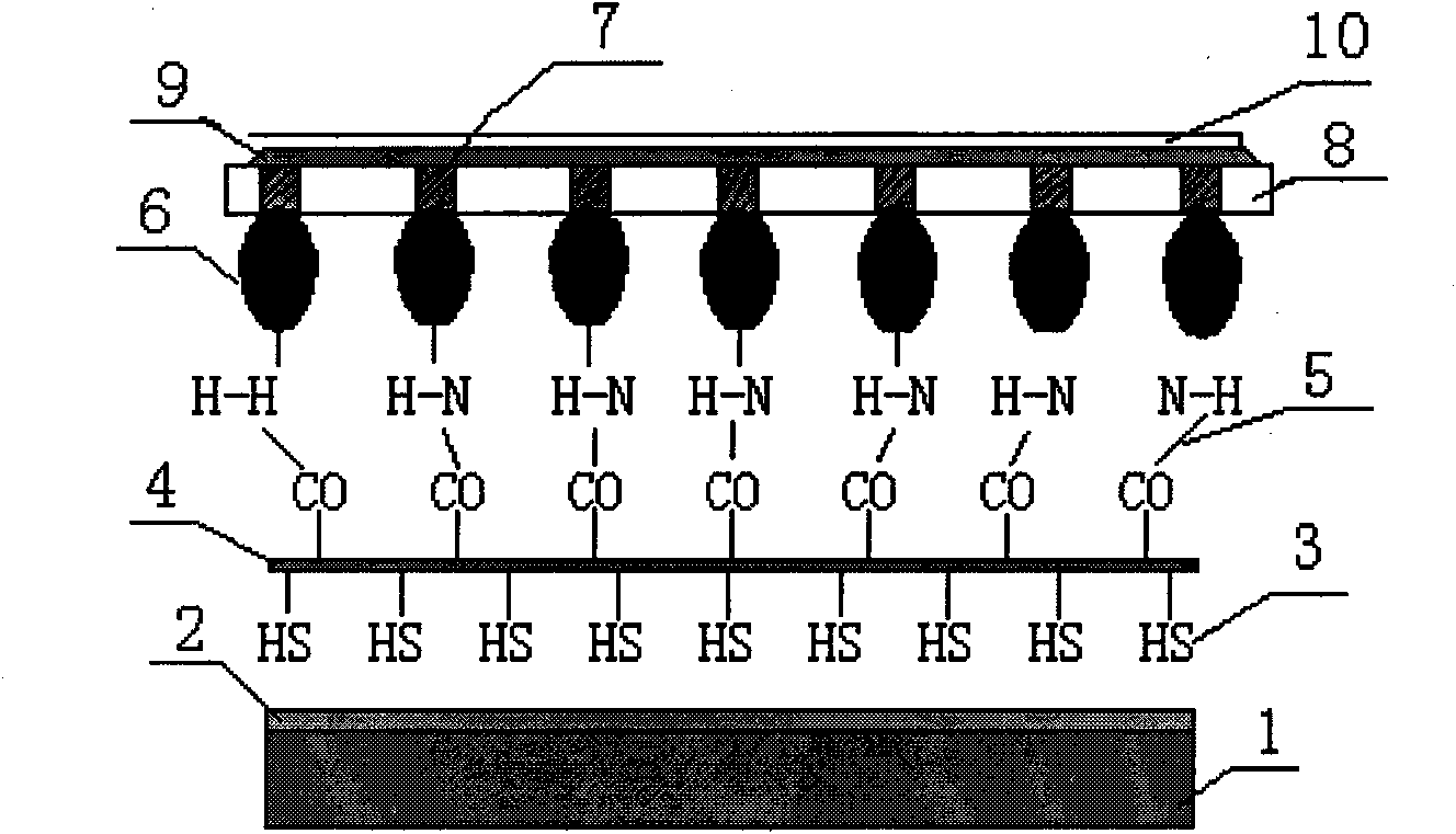
[0008] Specific Embodiment 1: In this embodiment, the method for manufacturing a protein-structured fast switching memristor array is manufactured according to the following steps: 1. A layer of gold with a thickness of 70-90 nm is fabricated on the upper surface of a silicon wafer by magnetron sputtering. 2. Immerse the silicon wafer coated with gold film into a solute concentration of 5×10 -3 The ethanol solution of mol / L 11-mercapto-1-undecanol was reacted for 5-7 hours to form a mercapto-hydrophilic surface on the surface of the gold film. The mass concentration is 70% to 90%; 3. The silicon chip with the mercapto group hydrophilic surface prepared in step 2 is immersed in an alkali ether solution of epichlorohydrin with a solute concentration of 0.6 to 0.8 mol / L and reacted for 3 to 5 hours, That is, an epoxy surface is formed on the hydrophilic surface, wherein the solvent of the alkali ether solution of epichlorohydrin consists of NaOH solution with a concentration of 0...

specific Embodiment approach 2

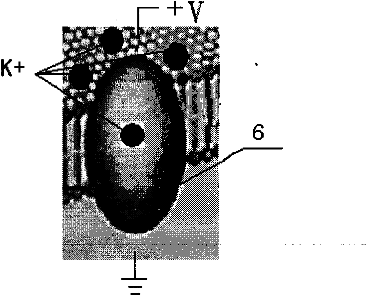
[0013] Specific embodiment 2: The difference between this embodiment and specific embodiment 1 is that in step 7, 60-100 mmol of K is added dropwise on the surface of the nanopore array film. + ionic liquid. Other steps and parameters are the same as those in Embodiment 1.

[0014] In this embodiment, different numbers of K + Ion-implanted protein-structured memristor cell switch arrays.

specific Embodiment approach 3

[0015] Specific embodiment three: the difference between this embodiment and specific embodiment one is that in step seven, 60 to 100 mmol of Na is added dropwise on the surface of the nanopore array film. + ionic liquid. Other steps and parameters are the same as those in Embodiment 1.

[0016] In this embodiment, a protein-structured memristor unit switch array with different numbers of Na+ ions implanted under the action of an external bias is obtained.


PUM


Abstract

A manufacturing method for a protein structure quick switch memristor array relates to the manufacturing method for protein structure memristor array. The manufacturing method solves the problems that the existing manufacturing method for a memristor model has low manufacturing cost and the prepared memristor manufacturing model has low on-off speed. The manufacturing method uses a method combining a micro electronic technique and a biochemistry technique for fixing bovine immunity globular protein on semiconductor material, prepares biology cell membranes, and then manufactures the protein structure quick switch memristor array; the preparation method for the nanometer structure memristor array is simple; the used raw materials have low price and low manufacturing cost; and the manufactured memristor array has quicker on-off speed.

Description

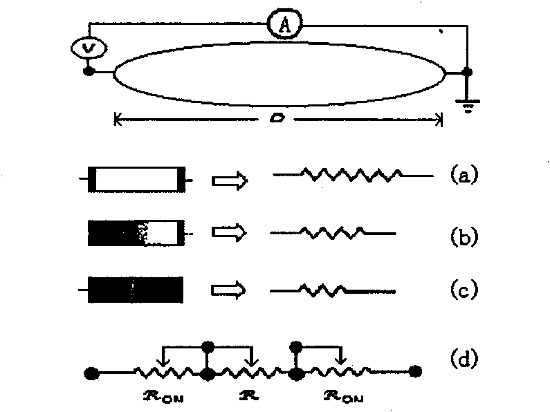
technical field [0001] The invention relates to a method for making a protein structure memristor array Background technique [0002] Dmitri B.StruK+ov, Gregory S.Snider, Duncan R.Stewart & R.Stanley Williams, researchers from Hewlett-Packard Laboratories in the United States, published a paper in the British "Nature" on May 1, 2008, claiming that , they have confirmed the fourth basic component in the circuit world - memristor, referred to as memristor (Memristor), and successfully designed a working memristor physical model, and applied for US patent US20080090337A1. Like making a sandwich, they made a nano-scale titanium dioxide semiconductor film TiO 2-x / TiO 2 Sandwiched between two nanowires made of platinum, making Pt / TiO 2-x / TiO 2 / Pt nanostructure, the trick to making memristor is to make its components only 5 nanometers in size, that is to say, it is only 1 / 10,000th as thin as a human hair. This existing memristor model is actually a non-linear resistor with ...

Claims


Application Information

Patent Timeline
Patent Type & Authority Applications(China)
IPC IPC(8): H01L21/8256H01L51/00H10K99/00
Inventor 温殿忠
Owner HEILONGJIANG UNIV
Why Eureka
Eureka Blog
Learn More