

Antiseptic filtering metal material by plating Cu and CeO2 on surface of copper wire mesh, and preparation and application thereof
A metal filtering and metal plating technology, which is applied in metal material coating process, filtration separation, sputtering plating, etc., can solve the problems of insufficient copper intake in the human body, bacterial breeding, etc., and achieve good sterilization and low cost. , the effect of large specific surface area
- Summary
- Abstract
- Description
- Claims
- Application Information
AI Technical Summary
Problems solved by technology
Method used
Image

Examples
Embodiment 1
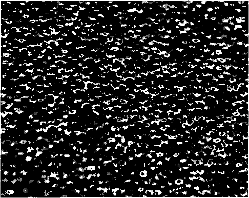
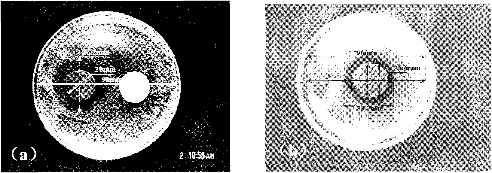
[0024] A copper film of 3 micrometers is deposited on the surface of the foam sponge material (about 550 micrometers in pore size) by ion sputtering coating method, so that the foam sponge material obtains electrical conductivity. Under the conditions of the composition ratio and process parameters shown in Table 1, electroplate copper film on the foam sponge material after conductive treatment. When the film thickness of the electroplating material is about 20 μm, take it out from the electroplating solution, wash it with water, and dry it in the air. , heated to 800°C for 3 hours under the protection of argon, and took it out after cooling down to room temperature, and removed the foam sponge in the grid frame to form a metal copper grid;
[0025] Table 1 Cu electroplating solution formula and process parameters
[0026] Components and process parameters
Content (g / L) or parameters
Components and parameters
Content (g / L) or parameters
Copper pyrop...
Embodiment 2
[0055] The difference from Example 1 is:
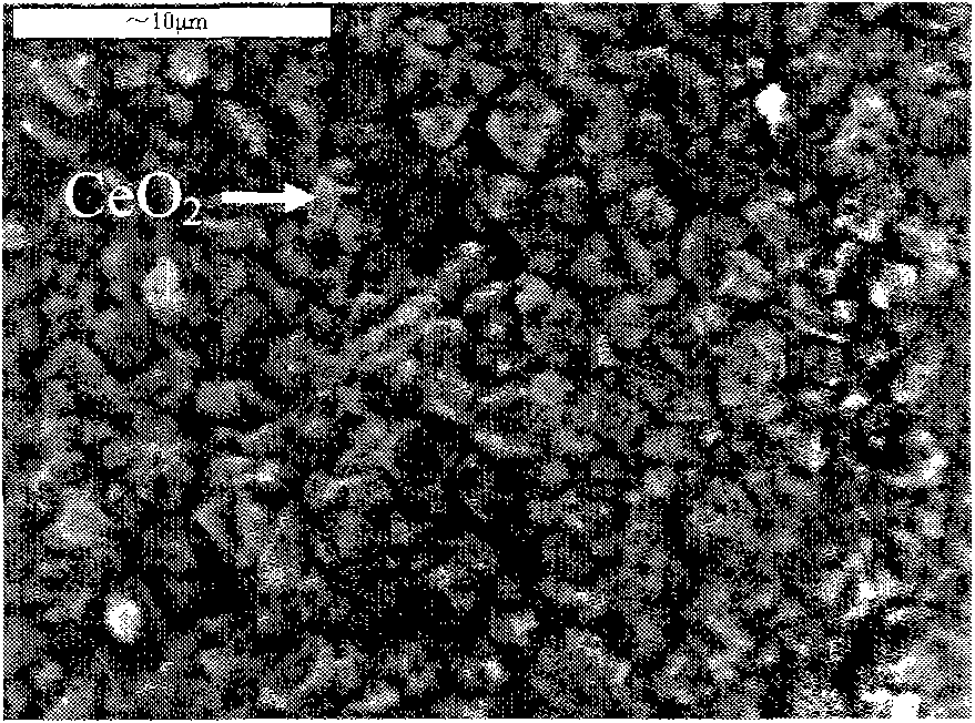
[0056] A 2-micron copper film is deposited on the surface of the foam sponge material (about 450 micrometers in pore size) by ion sputtering coating method, so that the foam sponge material obtains electrical conductivity. Under the conditions of composition ratio and process parameters shown in Table 1, electroplate copper film on the foam sponge material after conductive treatment. When the film thickness of the electroplating material is about 50 μm, take it out from the electroplating solution, wash it with water and dry it in the air. , heated to 850°C for 1 hour under the protection of argon, took it out after cooling down to room temperature, removed the foam sponge in the grid frame, and formed a metal copper mesh; finally, deposited 2.5 micron thick metal copper mesh on the surface of the prepared metal copper mesh Cu plus CeO 2 film, so that the supported metal (Cu+CeO 2 ) / Cu composite mesh antibacterial filter metal mater...
Embodiment 3
[0059] The difference from Example 1 is:
[0060] A 2.5-micron copper film is deposited on the surface of the foam sponge material (with a pore size of about 450 micrometers) by ion sputtering coating method, so that the foam sponge material obtains electrical conductivity. Under the conditions of the composition ratio and process parameters shown in Table 1, electroplate copper film on the foam sponge material after conductive treatment. When the film thickness of the electroplating material is about 23 μm, take it out from the electroplating solution, wash it with water, and dry it in the air. , heated to 700°C for 4 hours under the protection of argon, took it out after cooling down to room temperature, removed the foam sponge in the grid frame, and formed a metal copper grid; finally, deposited a 2-micron-thick metal copper grid on the surface of the prepared metal copper grid. Cu plus CeO 2 film, so that the supported metal (Cu+CeO 2 ) / Cu composite mesh antibacterial fi...
PUM
| Property | Measurement | Unit |
|---|---|---|
| thickness | aaaaa | aaaaa |
| thickness | aaaaa | aaaaa |
| pore size | aaaaa | aaaaa |
Abstract
Description
Claims
Application Information