Combined luminous element of electronic barrier layer

An electron blocking layer and light-emitting element technology, applied in electrical components, phonon exciters, laser parts, etc., can solve the problems of poor lattice quality and difficulty in increasing the hole concentration of aluminum gallium nitride, and achieve a reduction in stress. cumulative effect

Inactive Publication Date: 2010-02-03
ZHANJING TECH SHENZHEN +1
View PDF4 Cites 25 Cited by
  • Summary
  • Abstract
  • Description
  • Claims
  • Application Information

AI Technical Summary

Problems solved by technology

In addition, the higher the aluminum content, the worse the lattice quality, and it is relatively difficult to increase the hole concentration of AlGaN

Method used


Image

  • Combined luminous element of electronic barrier layer
  • Combined luminous element of electronic barrier layer
  • Combined luminous element of electronic barrier layer

Examples


Embodiment Construction

[0035] The direction of the present invention discussed here is a light emitting element. In order to provide a thorough understanding of the present invention, detailed structural elements will be set forth in the following description. Obviously, the practice of the invention is not restricted to specific details of the light-emitting elements known to those skilled in the art. On the other hand, well-known elements have not been described in detail in order not to unnecessarily limit the invention. Preferred embodiments of the present invention will be described in detail as follows, but in addition to these detailed descriptions, the present invention can also be widely implemented in other embodiments, and the scope of the present invention is not limited, with the scope of the following claims prevail.

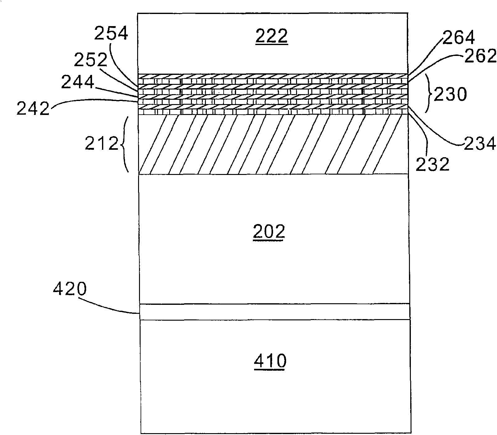
[0036] image 3 A schematic cross-sectional view of a combined electron-blocking layer light-emitting element according to a preferred embodiment of the present inven...


PUM


Abstract

The invention discloses a combined luminous element of an electronic barrier layer, which can be provided with an active luminous layer, an n-type gallium nitride layer, a p-type gallium nitride layer, and two III-V semiconductor layers with different energy gaps, wherein the semiconductor layers are periodically and repeatedly deposited on the active luminous layer as the electronic barrier layerwith higher potential barrier to obstruct excessive electronic active luminous layers. The combined luminous element can realize obstruction of electronic overflow through the electronic barrier layer to increase the composite probability of electrons and holes in the active luminous layer and discharge photons, and provides stress compensation through the combination of the III-V semiconductor layers with different crystal lattice sizes to reduce the accumulation of stress between the luminous element and the active luminous layer.

Description

technical field [0001] The invention relates to an electronic product, in particular to a light emitting element. Background technique [0002] During the operation of the light-emitting element, the phenomenon of electron overflow will not only reduce the luminous efficiency of the element, but also cause a rise in temperature and affect the service life of the element. Therefore, how to effectively reduce electron overflow is a very important link when manufacturing light-emitting elements. [0003] figure 1 A schematic cross-sectional view of a conventional light-emitting element using a gallium nitride-based semiconductor is shown. see figure 1 , a conventional light-emitting element has an n-type GaN layer 102 , an active light-emitting layer 112 , and a p-type GaN layer 122 . [0004] figure 2 show the basis figure 1 The energy diagram of the energy gap of each layer. in, figure 2 Depicted above, is the path energy taken by the electron. figure 2 Depicted b...

Claims


Application Information

Patent Timeline
Patent Type & Authority Applications(China)
IPC IPC(8): H01L33/00H01S5/343
Inventor 吴芃逸黄世晟涂博闵叶颖超林文禹徐智鹏詹世雄
Owner ZHANJING TECH SHENZHEN
Why Eureka
Try Eureka