Bidirectional trigger diode chip production method

A two-way triggering and diode technology, applied in semiconductor/solid-state device manufacturing, electrical components, circuits, etc., can solve problems such as affecting product reliability, single packaging form, inconvenient production volume, etc., to avoid stress, reduce production costs, and reduce operation. handy effect

Active Publication Date: 2010-02-17
NANTONG MINICHIP MICRO ELECTRONICS
View PDF0 Cites 20 Cited by
  • Summary
  • Abstract
  • Description
  • Claims
  • Application Information

AI Technical Summary

Problems solved by technology

[0002]The more advanced technology in the manufacture of bidirectional trigger diode chips today is to use a low-resistivity P+ type double-grinding single chip for preparation, and the process steps are: pickling , cleaning, diffusion, grooving, glass passivation, electroplating, alloying, electroplating, testing, scribing, and splitting. The disadvantage of this method is that the breakdown voltage of the product is determined by the resistivity of the selected material and cannot be adjusted; The electrodes of the product are formed by electroplating, and the electrode materials on the fron

Method used


Image

  • Bidirectional trigger diode chip production method
  • Bidirectional trigger diode chip production method

Examples


Embodiment Construction

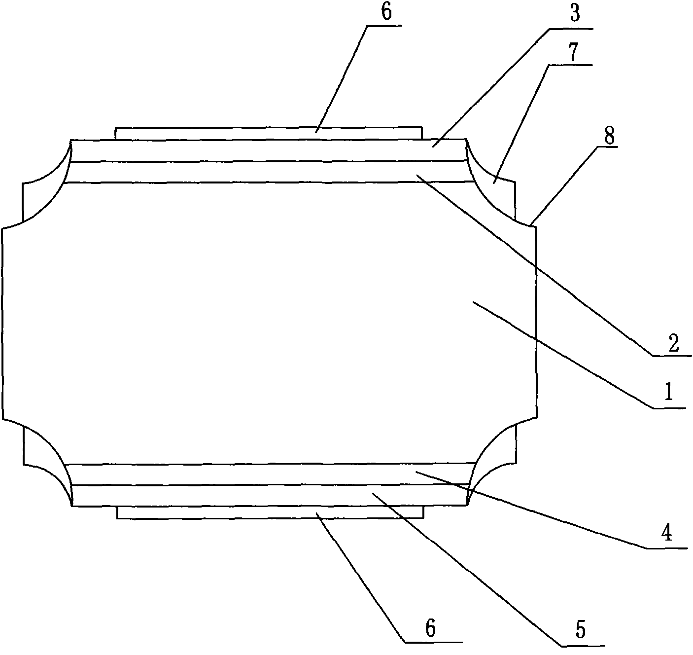
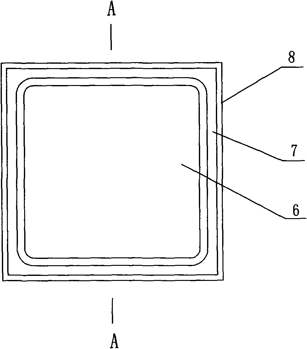
[0020] The bidirectional trigger diode is a special semiconductor device, and its important electrical characteristic parameters include forward and reverse breakdown voltage, dynamic rebound voltage and conduction voltage drop. The internal structure of the chip is a transistor structure, but there is no base lead, and the emitter and collector can be exchanged arbitrarily. Based on the transistor principle, by adjusting the first and second diffusion concentration and junction depth, a suitable β 0 , to ensure the trigger voltage and rebound voltage of the product. The thickness of the selected silicon wafer material must ensure a small conduction voltage drop.

[0021] this invention figure 1 The P-type impurity diffusion in the 2nd region and 4th region is completed in the same diffusion process, figure 1 The diffusion of N+ type impurities in the 3rd and 5th regions is also completed in the same diffusion process, which ensures the symmetry of the forward and reverse b...


PUM

PropertyMeasurementUnit
Resistivityaaaaaaaaaa

Abstract

The invention discloses a bidirectional trigger diode chip production method, belonging to the filed of the semiconductor device production technology. The independent bidirectional trigger diode chipis produced according to the following processing steps of silicon slice cleaning, first-time diffusing, second-time cleaning, second-time diffusing, first-time photoetching, table-top forming, glasspassivating, second-time photoetching, two-surface coating, third-time photoetching, fourth-time photoetching and final scribing. The breakdown voltage of the bidirectional trigger diode chip can beadjusted in a large range according to the requirement of the user; the bidirectional trigger diode chip can be packaged in various ways so as to meet the requirements of different users and circuits;the reliability of the bidirectional trigger diode chip is improved due to the fourth-time photoetching process; and the bidirectional trigger diode chip can be used for the production of the four-inch silicon slice so that the production efficiency of the four-inch silicon slice is improved and the finished product ratio is high.

Description

technical field [0001] The invention relates to a method for manufacturing a semiconductor device, in particular to a method for manufacturing a bidirectional trigger diode. Background technique [0002] The more advanced technology in today's bidirectional trigger diode chip manufacturing is to use a low-resistivity P+ type double-grinding single chip for preparation. The process steps are: pickling, cleaning, diffusion, groove, glass passivation, electroplating, alloying , electroplating, testing, scribing, and splitting. The disadvantages of this method are: the breakdown voltage of the product is determined by the resistivity of the selected material and cannot be adjusted; the electrodes of the product are formed by electroplating, and the electrodes on the front and back sides The material is the same, so only axial packaging can be used, and the packaging form of the product is single; scribing directly on the glass passivation layer will affect the reliability of the...

Claims


Application Information

Patent Timeline
IPC IPC(8): H01L21/329H01L21/228H01L21/22H01L29/02
Inventor 申云周明
Owner NANTONG MINICHIP MICRO ELECTRONICS
Why Eureka
Try Eureka