Method for controlling specific resistance of gallium-doped Czochralski silicon in crystal growth process

A crystal growth and resistivity technology, applied in the field of solar cell materials, can solve problems such as the inability to prepare high-efficiency solar cells, and achieve the effects of easy large-scale application, increased utilization, and reduced manufacturing costs

Inactive Publication Date: 2010-02-24
ZHEJIANG UNIV
View PDF0 Cites 39 Cited by
  • Summary
  • Abstract
  • Description
  • Claims
  • Application Information

AI Technical Summary

Problems solved by technology

For the remaining 40-50% silicon crystals, the current conventional cell technology cannot produce high-efficiency solar cells

Method used


Image

  • Method for controlling specific resistance of gallium-doped Czochralski silicon in crystal growth process
  • Method for controlling specific resistance of gallium-doped Czochralski silicon in crystal growth process
  • Method for controlling specific resistance of gallium-doped Czochralski silicon in crystal growth process

Examples


Embodiment 1

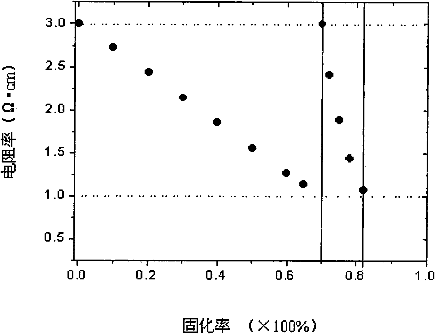
[0019] 50kg of polysilicon was put into a quartz crucible, and 1.365g of gallium was doped at the same time (making the target resistivity of the head of gallium-doped Czochralski silicon single crystal be 3Ω·cm). Under the protection of argon, polysilicon was melted at 1410°C, and gallium was melted into the polysilicon solution. The crystal growth parameters were adjusted as usual, and a Czochralski silicon single crystal with a diameter of 150 mm was grown at a growth rate of 1.2 mm / min. When the crystal growth length reached 80 cm, 2.25 mg of phosphorus was added to the remaining silicon solution through the dopant dopant device, and then the silicon single crystal growth continued, and it was finished when the solidification rate reached 82%. Samples were taken at different parts of the grown crystal, and then the axial distribution of the resistivity of the raw crystal was tested by the four-probe method, as shown in the attached figure 1 shown. It can be seen that the ...

Embodiment 2

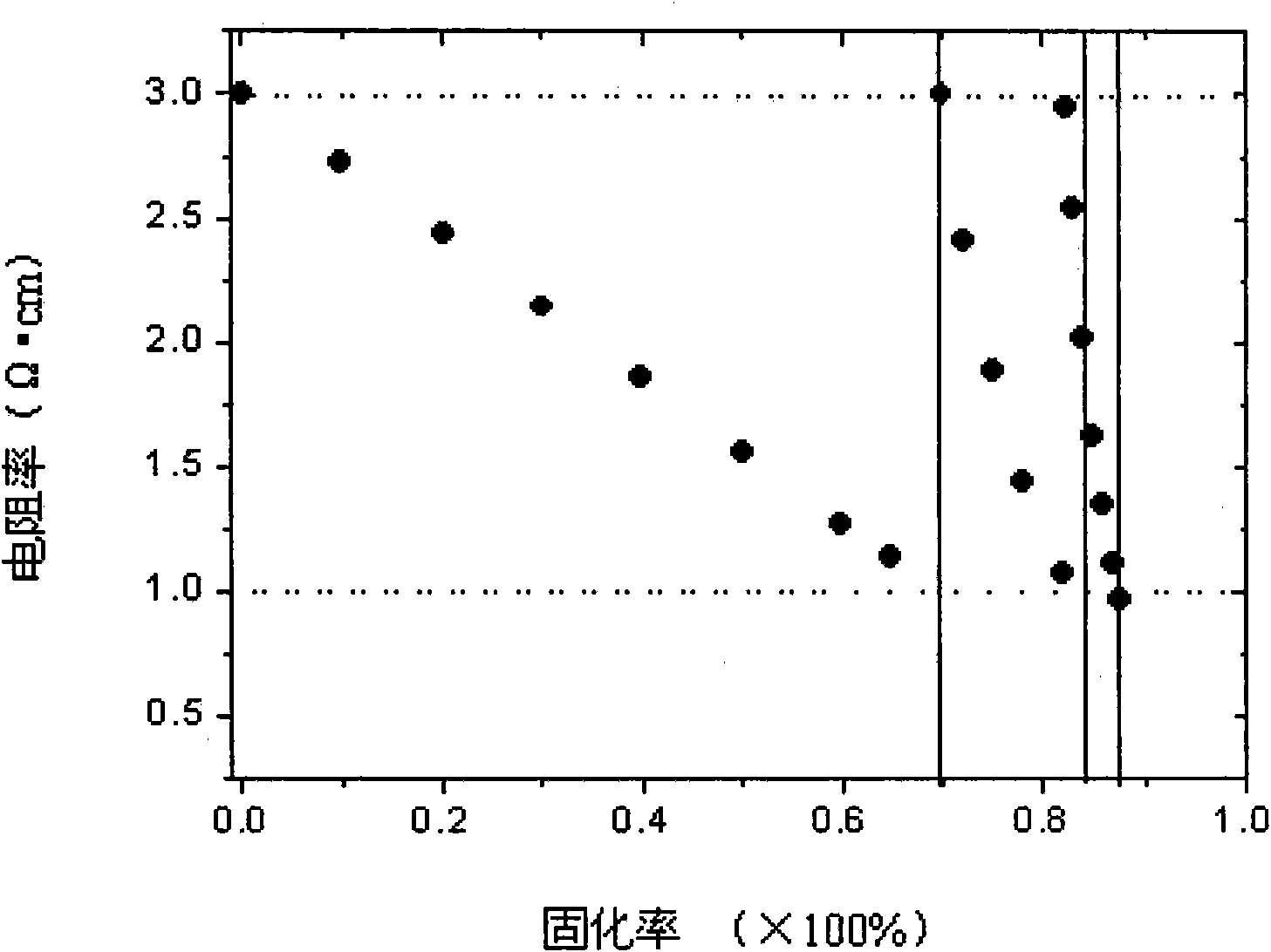
[0021] 50kg of polysilicon was put into a quartz crucible, and 1.365g of gallium was doped at the same time (making the target resistivity of the head of gallium-doped Czochralski silicon single crystal be 3Ω·cm). Under the protection of argon, polysilicon was melted at 1410°C, and gallium was melted into the polysilicon solution. The crystal growth parameters were adjusted as usual, and a Czochralski silicon single crystal with a diameter of 150 mm was grown at a growth rate of 1.2 mm / min. When the crystal growth length reached 80 cm, 2.25 mg of phosphorus was added into the crucible through the dopant dopant device, dissolved into the remaining silicon melt, and then continued to grow silicon single crystal. When the crystal length reached 94 cm, 1.35 mg of phosphorus was added to the crucible through the dopant dopant device, and dissolved into the remaining silicon melt. Finish when the curing rate reaches 88%. Samples were taken at different parts of the grown crystal, a...

Embodiment 3

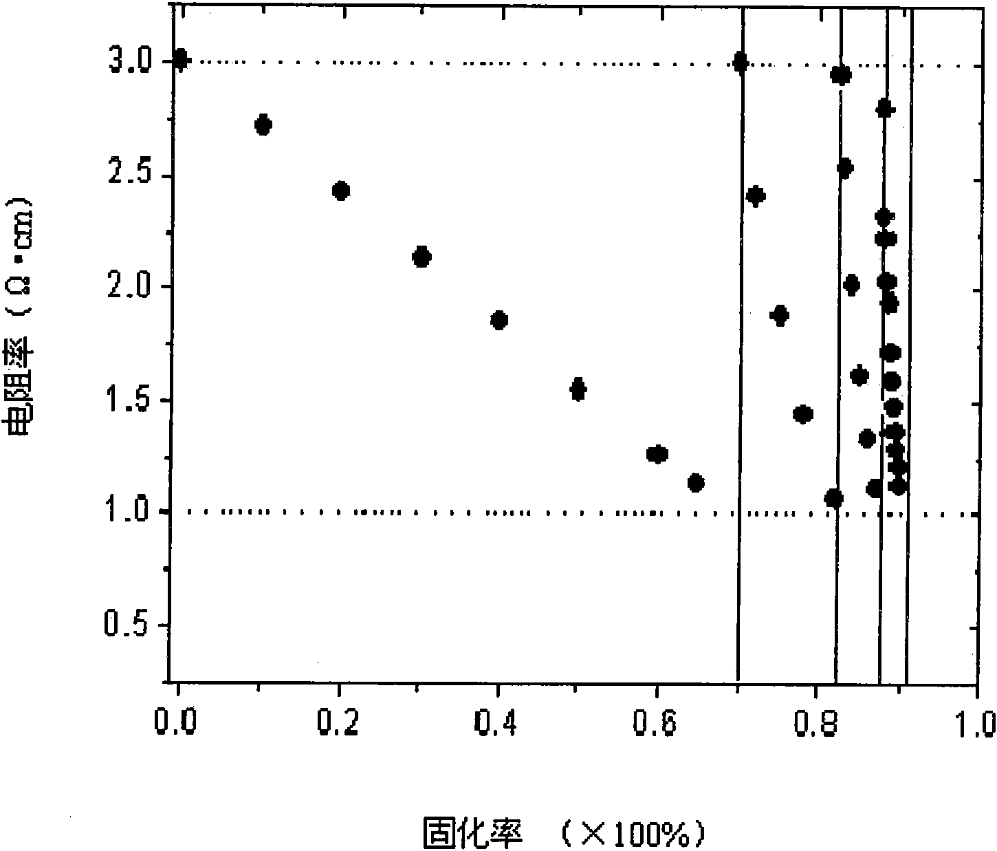
[0023] 50kg of polysilicon was put into a quartz crucible, and 1.365g of gallium was doped at the same time (making the target resistivity of the head of gallium-doped Czochralski silicon single crystal be 3Ω·cm). Under the protection of argon, polysilicon was melted at 1410°C, and gallium was melted into the polysilicon solution. The crystal growth parameters were adjusted as usual, and a Czochralski silicon single crystal with a diameter of 150 mm was grown at a growth rate of 1.2 mm / min. When the crystal growth length reached 80 cm, 2.25 mg of phosphorus was added into the crucible through the dopant dopant device, and dissolved into the remaining silicon melt to continue growing silicon single crystal. When the crystal length reaches 94cm, add 1.35mg of phosphorus into the crucible through the dopant dopant device, dissolve into the remaining silicon melt, and continue to grow silicon single crystal. When the crystal length reaches 94cm, add 1.35mg of phosphorus into the c...


PUM

PropertyMeasurementUnit
electrical resistivityaaaaaaaaaa

Abstract

The invention discloses a method for controlling the specific resistance of gallium-doping Czochralski silicon in the crystal growth process, which comprises the following steps: melting multi-crystalsilicon in vacuum or under the protection of argon, melting gallium in the silicon solution to form a gallium-doping silicon solution, and growing the single crystal of the Czochralski silicon; in the crystal growth process, when the specific resistance of the crystal is 1.2-1.0 omega cm, doping the n type dopant-phosphorus with certain concentration in the residual gallium-doping silicon solution to form a phosphorus and gallium-doped silicon solution for continuously growing, and enabling the specific resistance of the crystal to be regulated to 3.0 omega cm again; and when the curing ratioof the crystal reaches 80-90%, stopping the growth. The phosphorus doping process in the residual gallium-doped silicon solution can be carried out many times. The invention can control the specificresistance of the back half part of the single crystal of the gallium-doped Czochralski silicon in the range of 1-3 omega cm to be favorable for increasing the utilization ratio of silicon materials in the process of preparing high-efficiency solar batteries, thus the manufacturing cost of the high-efficiency batteries is greatly reduced, and the method has simple operation and can be easily applied to the photovoltaic industry in a large scale.

Description

technical field [0001] The invention belongs to the field of solar cell materials, in particular to the growth technology of gallium-doped Czochralski silicon single crystal for solar cells. Background technique [0002] Solar energy is an inexhaustible clean energy. Using the photoelectric conversion characteristics of semiconductor materials, it can be prepared into solar cells, which can convert solar energy into electrical energy. [0003] Czochralski silicon single crystal is one of the main materials for producing solar cells. In traditional solar photovoltaic technology, boron-doped Czochralski silicon single crystal is widely used in the preparation of solar cells. However, due to the replacement of boron atoms in the boron-doped Czochralski silicon single crystal and the oxygen atoms in the single crystal silicon, under the irradiation of sunlight, due to the injection of minority carriers, oxygen will combine with boron to form a boron-oxygen complex. . The boro...

Claims


Application Information

Patent Timeline
Patent Type & Authority Applications(China)
IPC IPC(8): C30B15/02C30B15/20
Inventor 余学功杨德仁
Owner ZHEJIANG UNIV
Why Eureka
Try Eureka