
Semiconductor device and method for fabricating same

A manufacturing method and semiconductor technology, applied in the direction of semiconductor devices, electrical solid devices, electrical components, etc., can solve the problems of high manufacturing cost and slow coating rate of epoxy resin layer, and achieve improved thickness uniformity, high production rate, The effect of reducing manufacturing costs

Inactive Publication Date: 2010-03-03
VISERA TECH CO LTD +1
View PDF0 Cites 12 Cited by
  • Summary
  • Abstract
  • Description
  • Claims
  • Application Information

AI Technical Summary

Problems solved by technology

However, the coating rate of the epoxy layer is slow and the manufacturing cost is high

Method used


Image

  • Semiconductor device and method for fabricating same
  • Semiconductor device and method for fabricating same
  • Semiconductor device and method for fabricating same

Examples


Embodiment Construction

[0018] Examples of the present invention are described below. The purpose of this description is to provide a general concept of the present invention and not to limit the scope of the present invention. The protection scope of the present invention should be determined by the claims.

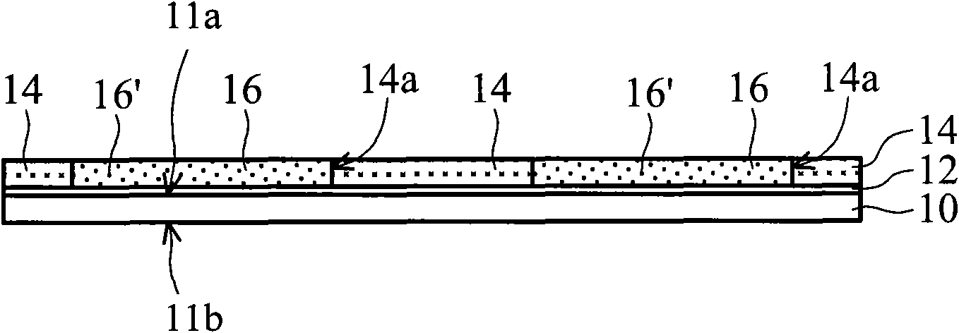
[0019] Figure 2D , 3D , 4D respectively show the cross-sectional schematic diagrams of LED devices according to different embodiments of the present invention, wherein Figure 3D and 4D and Figure 2D The same parts are used in , and the relevant descriptions are omitted. Please refer to Figure 2D , the LED device includes a semiconductor substrate 200, such as a silicon substrate or other known semiconductor substrates, which has a cavity 100a. The semiconductor substrate 200 may include various components such as transistors, resistors and other known semiconductor components. In order to simplify the drawings, individual components are not shown here.

[0020] At least two separat...


PUM


Abstract

The invention discloses a semiconductor device and a method for fabricating the same. The semiconductor device comprises a semiconductor substrate, a light-emitting diode chip disposed in a cavity ofthe semiconductor substrate, at least two isolated outer wiring layers disposed on the bottom surface of the semiconductor substrate and electrically connected to the light-emitting diode chip, serving as input terminals and a lens module adhered to the top surface of the semiconductor substrate to cap the cavity, in which the lens module comprises a molded lens and a transparent conductive layercoated with a fluorescent material under the molded lens. The invention can improve the thickness uniformity of the fluorescent layer, moreover, since the fluorescent layers are formed by electrophoresis and the LED devices are packaged by a wafer level package, high production rate can be obtained and manufacturing costs can be reduced.

Description

technical field [0001] The present invention relates to a light-emitting diode (light-emitting diode, LED) device, in particular to a light-emitting diode device having a lens module of fluorescent material deposited by electrophoresis, and the manufacture of the light-emitting diode device method. Background technique [0002] Light emitting diode (LED) devices are solid state light sources and have been used for many years. LED devices emit light through the combination of electron-hole pairs at the p-n junction of semiconductor materials when they are forward biased. Compared with traditional lamps, LED devices have the advantages of low power consumption and long service life. In particular, white LED devices have high color rendering index (CRI), making them one of the most widely accepted lighting devices. [0003] White LED devices can be formed by mixing red, green, and blue light using red LED chips (chips / dies), green LED chips, and blue LED chips. However, the...

Claims


Application Information

Patent Timeline
Patent Type & Authority Applications(China)
IPC IPC(8): H01L33/00
CPCH01L33/507H01L33/44H01L33/486H01L2933/0091H01L2924/10253H01L2224/48091H01L33/62H01L33/58H01L2224/48227H01L2924/00014H01L2924/00
Inventor 林孜翰翁瑞坪林孜颖傅国荣
Owner VISERA TECH CO LTD
Learn More