Organic electroluminescent device capable of forming spin-polarized injection
An electroluminescent device and spin-polarized technology, which is applied in the direction of electric solid-state devices, electrical components, semiconductor devices, etc., can solve the problems that cannot be broken and limit the external quantum efficiency of the device, and achieve the improvement of luminous brightness and current efficiency, The effect of increasing the scale
- Summary
- Abstract
- Description
- Claims
- Application Information
AI Technical Summary
Problems solved by technology
Method used
Image
Examples
Embodiment 1
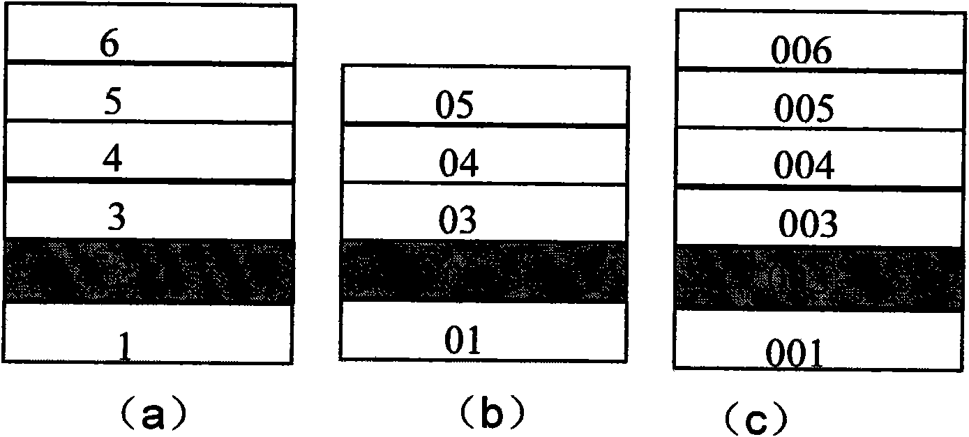
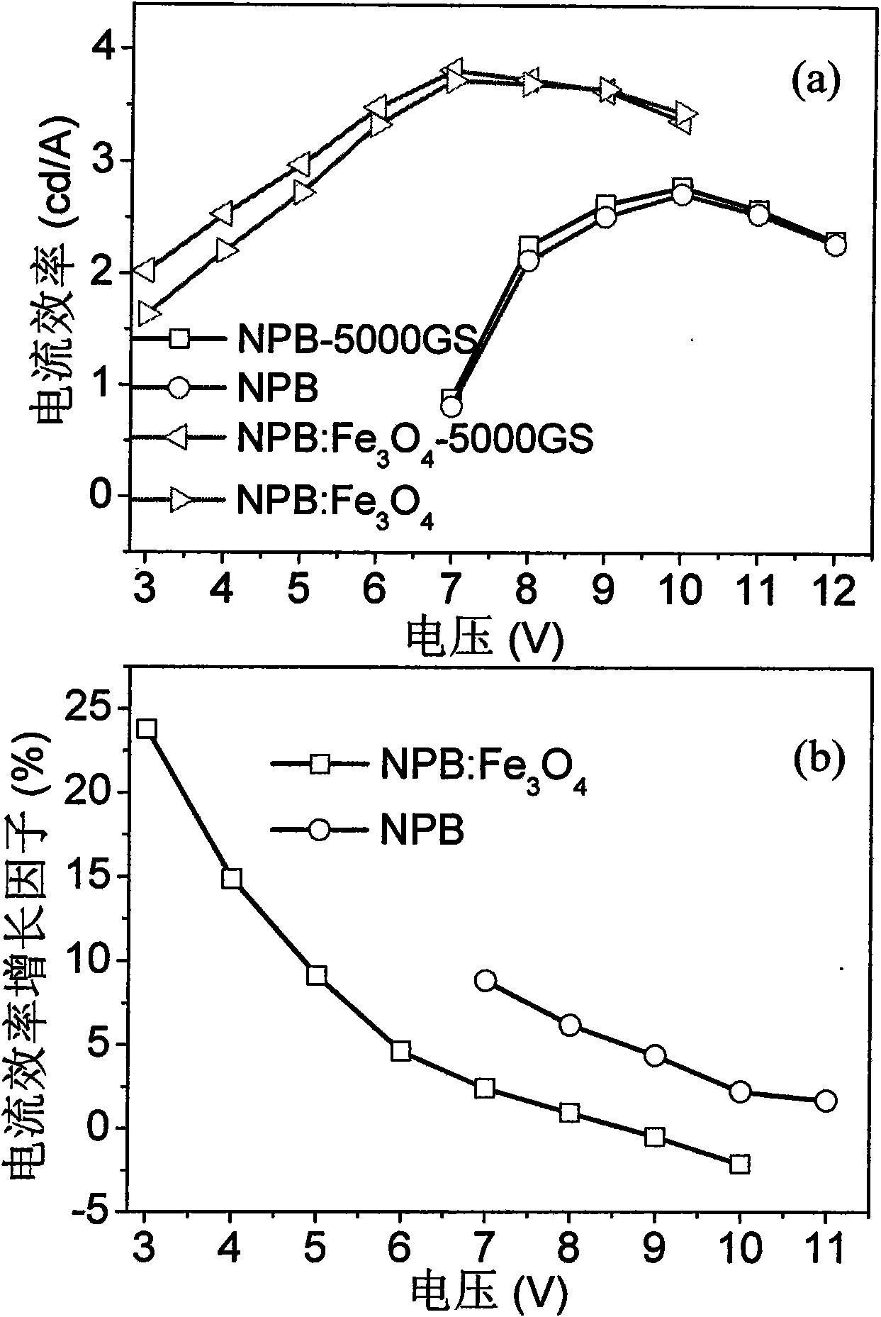
[0037] Based on Fe 3 o 4 Research and test of spin-polarized magnetic field effect of doped hole transport layer NPB device, device structure ITO / NPB: Fe 3 o 4 (doping ratio is 2:1, 25nm) / NPB(15nm) / Alq 3 (50nm) / LiF(1nm) / Al(100nm), such as figure 1 As shown in the device structure II, the comparison structure is ITO / NPB(40nm) / Alq 3 (50nm) / LiF(1nm) / Al.
[0038] The ITO glass substrate was scrubbed with acetone cotton ball and ethanol cotton ball in turn, and then ultrasonicated with acetone solution, ethanol solution, and deionized water for 10 minutes, and then on the cleaned ITO glass substrate, the multi-source organic molecular beam Each functional layer is grown sequentially in the deposition system, and the vacuum degree of the system is maintained at 4×10 -4 Around Pa, the hole transport layer uses dopant Fe 3 o 4 The method of co-evaporating with the host material NPB, that is, the dopant and the host material are evaporated and deposited on the substrate at the ...
Embodiment 2
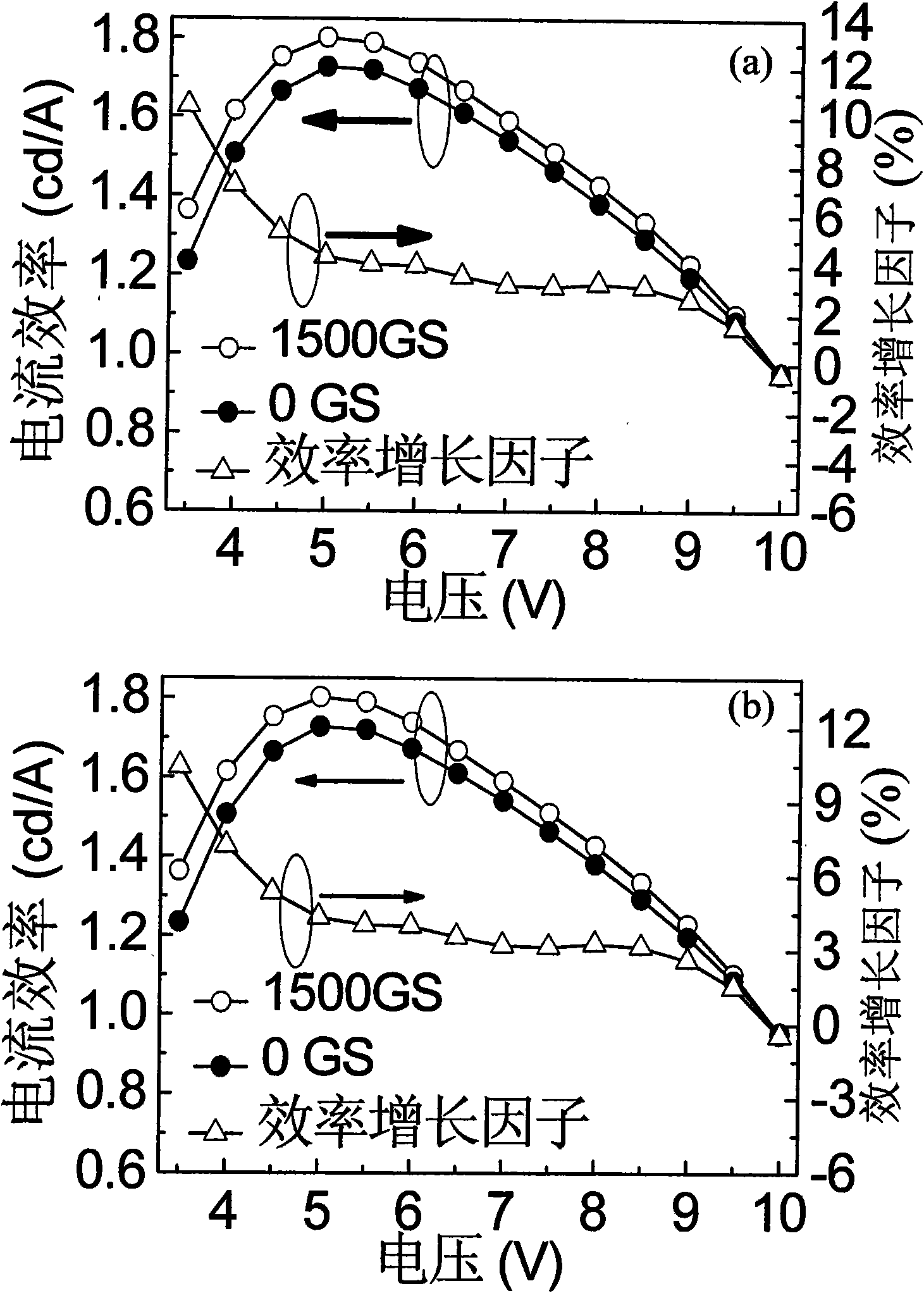
[0044] Based on Fe 3 o 4 Test and analysis of the spin-polarized magnetic field effect of a blue-light organic electroluminescence device as an anode buffer layer. Device structure such as figure 1 As shown in the device structure III in , 002 uses ITO, and 003 uses Fe with high spin polarizability 3 o 4 , NPB is selected for 004, Bphen is selected for 005, LiF / AL is selected for 006, and the specific structural parameters are as follows: ITO / Fe 3 o 4 / NPB(30nm) / Bphen(60nm) / LiF(1nm) / AL(100nm), the contrast structure is ITO / NPB(30nm) / Bphen(60nm) / LiF(1nm) / AL(100nm), in which NPB is used as the luminescent layer, Bphen is a hole blocking layer and also serves as an electron transport layer, which can effectively confine the injected carriers in the light-emitting layer for composite light emission, and the anode buffer layer Fe 3 o 4 The thickness of the device varies from 0nm to 10nm, and the preparation method of the device is the same as in Example 1. The test method i...
PUM
 Abstract
Description
Claims
Application Information


