Metal films, methods for production thereof, methods for production of laminated electronic components, and laminated electronic components

A metal film and manufacturing method technology, applied in the field of laminated electronic components, can solve the problems of the decrease of the electrostatic capacity of the laminated ceramic capacitor, the reduction of the effective area of ​​the conductor layer, the interruption and the void of the conductor layer, etc., so as to suppress the structural defects such as interruption and void, The effect of increasing the effective area and suppressing shrinkage

Inactive Publication Date: 2010-03-31
KYOCERA CORP
View PDF3 Cites 1 Cited by
  • Summary
  • Abstract
  • Description
  • Claims
  • Application Information

AI Technical Summary

Problems solved by technology

If Ni is segregated like this 3 S 2 Metal films of intermetallic compounds such as are used as conductor patterns, then as Figure 5 As shown, the end portion of the conductor layer 55 formed inside the multilayer ceramic capacitor shrinks, and a void 59 is easily formed between the end portion and the ceramic layer 57. Therefore, there is a problem that the thermal shock resistance test cannot be performed due to the void. gain reliability
However, if an industrial large-scale production firing furnace such as a tunnel-type continuous furnace is used and a large amount of firing is performed at the same time, since the temperature difference in the furnace is large compared with the experimental furnace, the firing temperature is low. For the samples fired in the region, the shrinkage of the end of the conductor layer decreases after firing, while the shrinkage of the end of the conductor layer becomes larger for the samples fired in the region with a high firing temperature, and at the same time, the conductor layer is prone to occur. Structural defects such as layer interruptions and voids
Therefore, the effective area of ​​the conductor layer is reduced, and as a result, there is a problem that the electrostatic capacity of mass-produced multilayer ceramic capacitors decreases.

Method used


Image

  • Metal films, methods for production thereof, methods for production of laminated electronic components, and laminated electronic components
  • Metal films, methods for production thereof, methods for production of laminated electronic components, and laminated electronic components
  • Metal films, methods for production thereof, methods for production of laminated electronic components, and laminated electronic components

Examples


Embodiment 1

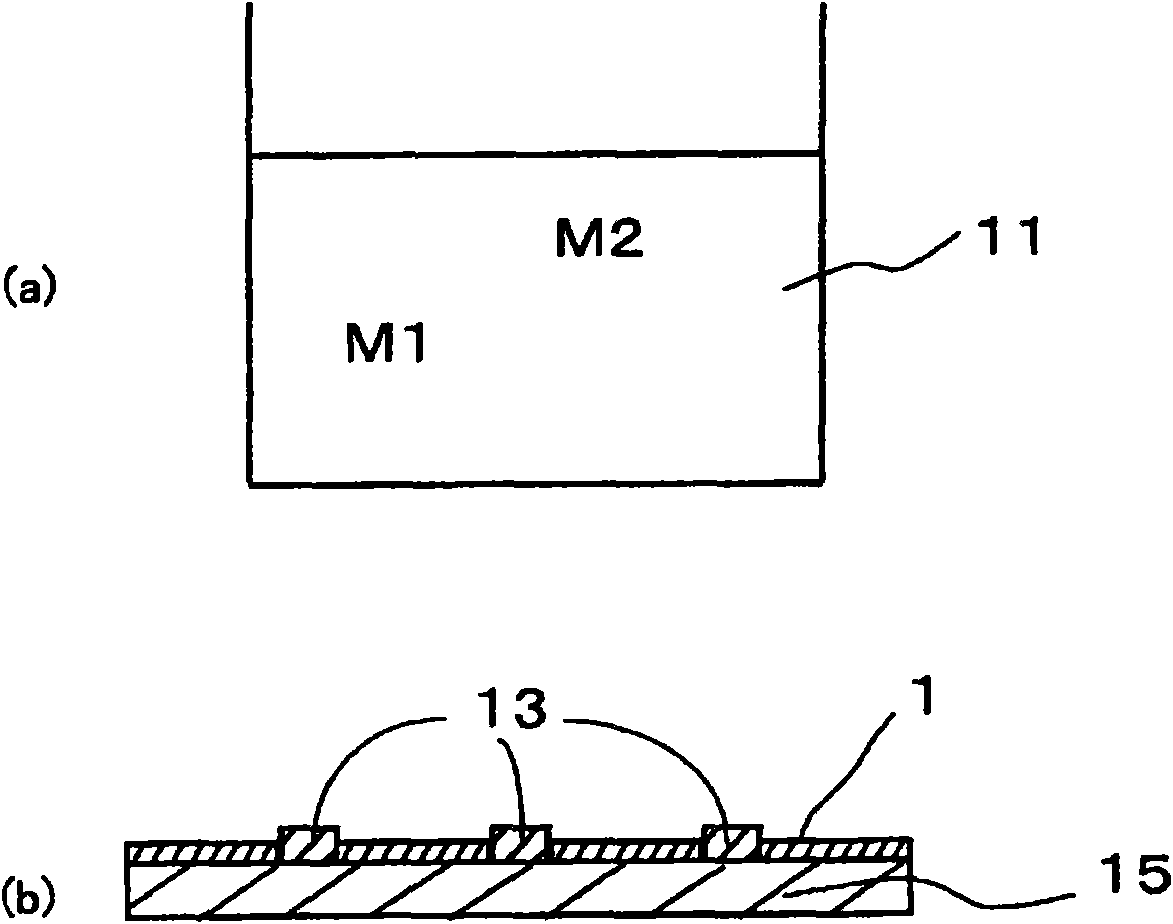
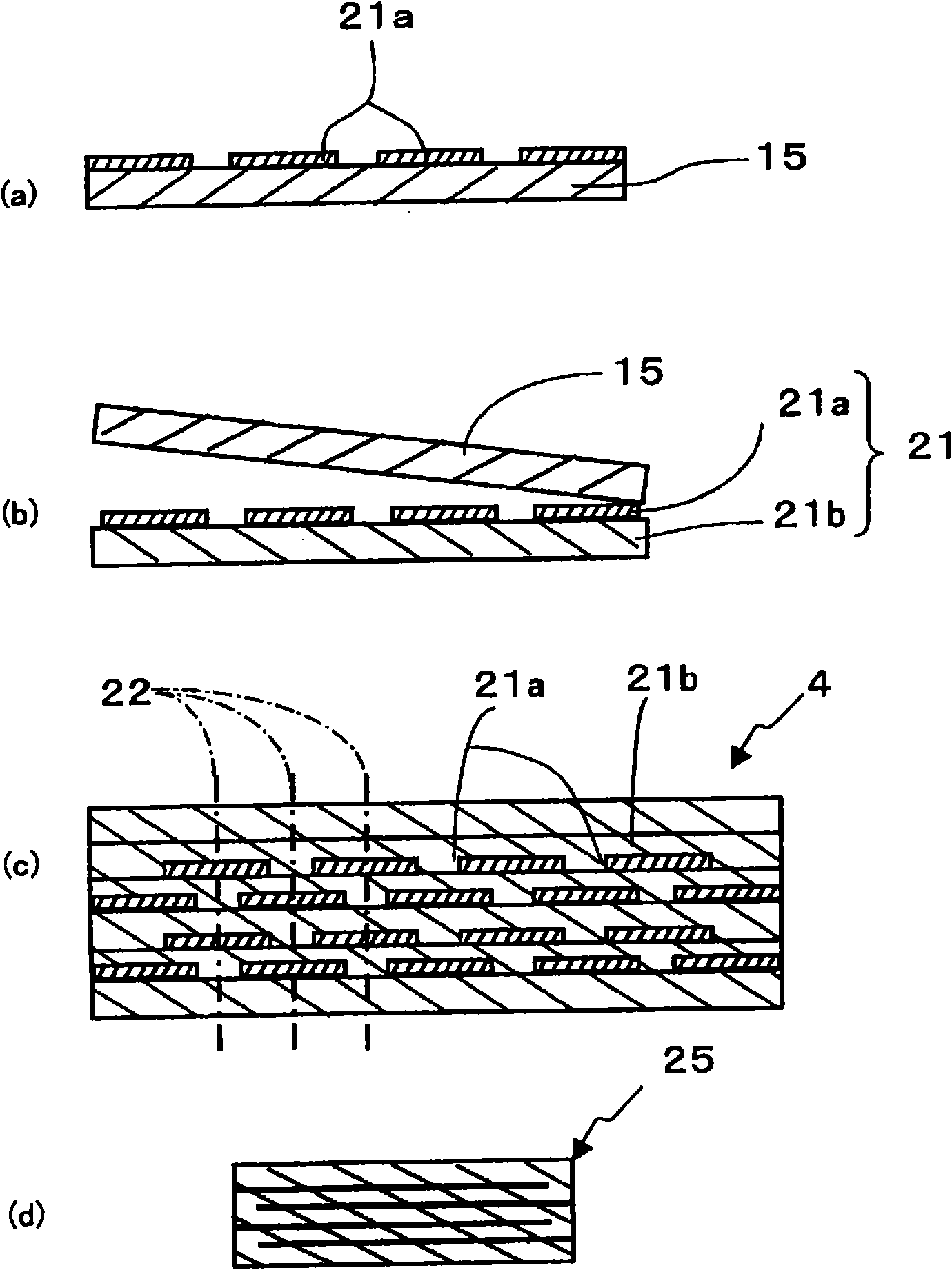
[0064] Regarding the metal film 21a and the multilayer electronic component of the present invention, a multilayer ceramic capacitor was fabricated and evaluated. First, a mirror-finished stainless steel substrate was used as a base material, and a photosensitive resist resin was applied to the surface to form a resist pattern. The resist pattern is a rectangular pattern arranged in a plurality of zigzags. The size of one pattern is 5 mm on the long side and 1.5 mm on the short side.

[0065] Next, electroplating was performed with a Ni plating solution 11 containing Mn and group 3A to 6A elements to form a Ni plating film with a thickness of 0.3 μm having a predetermined content of these added elements on a substrate made of stainless steel.

[0066] At this time, sulfuric acid ions containing, for example, group 3A to 6A elements are dissolved in the plating bath, and Mn is dissolved in manganese sulfate and electrolyzed in combination with a Ni anode. The concentration ad...

Embodiment 2

[0089] Next, the multilayer ceramic capacitors of sample Nos. 2 to 7 in Example 1 were fired within the firing temperature range shown in Table 2 to prepare samples, and the same evaluation was performed. Table 2 shows the results.

[0090] [Table 2]

[0091]

[0092] * represents samples outside the scope of the present invention.

[0093] Nos. 12 to 16, which are samples using the metal film 21a of the present invention, have a firing temperature of 1150 to 1200°C, exhibit capacitance equivalent to the characteristics at 1170°C, and have a high failure rate in the thermal shock resistance test. Below 1 / 100.

[0094] On the other hand, sample No. 11 using a composite metal powder other than the present invention had a firing temperature of 1150 to 1200°C, a capacitance as low as 9 μF or less, or a large number of delaminations in the thermal shock resistance test. In addition, There are also differences depending on the firing temperature.


PUM

PropertyMeasurementUnit
melting pointaaaaaaaaaa
thicknessaaaaaaaaaa
thicknessaaaaaaaaaa

Abstract

A metal film containing Ni as a main component and Mn and at least one element selected from the group consisting of the elements of Groups 3A, to 6A of the periodic table includes a central part anda peripheral part in which Mn and the element selected from the group consisting of the elements of Groups 3A to 6A of the periodic table are present in a concentration higher in the peripheral part than that in the central part. The metal film used as a conductor layer can have an increased melting point at the peripheral part and thus can be prevented from shrinking during heating. The metal film used as a conductor layer in electronic components and the like can be prevented from plastically deforming or shrinking during heating so that the conductor layer can have a large effective area and high adhesion to ceramic layers.

Description

technical field [0001] The present invention relates to a kind of metal film and its manufacturing method, and the manufacturing method of laminated electronic component and laminated electronic component, especially relate to the metal film with Ni as main component and its manufacturing method, also this metal film is used as A method of manufacturing a multilayer electronic component to which a conductor layer is applied, and a multilayer electronic component. Background technique [0002] In recent years, multilayer ceramic capacitors, which are representative examples of multilayer electronic components, have been required to reduce the thickness of the dielectric layer as the ceramic layer and thinner the inner electrode layer as the conductor layer in response to the demand for smaller size and higher capacity. For example, as the conductive pattern of the internal electrode layer, its formation method is not only the method of forming a thin film on a thin film by a ...

Claims


Application Information

Patent Timeline
Patent Type & Authority Applications(China)
IPC IPC(8): C25D7/00C22C19/03C25D3/56C25D5/00H01G4/12H01G4/30
CPCC22C13/00C25D5/50C25D5/48C22C19/03H01G4/30C25D3/562H01G4/0085C25D7/00H01G4/008C25D5/00Y10T428/24917
Inventor 山口胜义
Owner KYOCERA CORP
Why Eureka
Try Eureka