High-low voltage device for plasma display driving chip and preparation method

A display drive, high and low voltage technology, applied in the field of row address driver chips and column address driver chips for ion displays, can solve problems such as insufficient reliability, achieve good reliability performance, high isolation reliability, and anti-latch performance Good results

Active Publication Date: 2010-05-26
SUZHOU POWERON IC DESIGN
View PDF0 Cites 17 Cited by
  • Summary
  • Abstract
  • Description
  • Claims
  • Application Information

AI Technical Summary

Problems solved by technology

The traditional isolation method is mainly based on bulk silicon PN junction isolation or single-slot isolation, in which the PN isolation structure occupies more than 20% of the chip area, while the single-slot isolation occupies a small area of ​​the chip and can be controlled within 5%. However, there are still deficiencies in the reliability of the isolation

Method used


Image

  • High-low voltage device for plasma display driving chip and preparation method
  • High-low voltage device for plasma display driving chip and preparation method
  • High-low voltage device for plasma display driving chip and preparation method

Examples


Embodiment 1

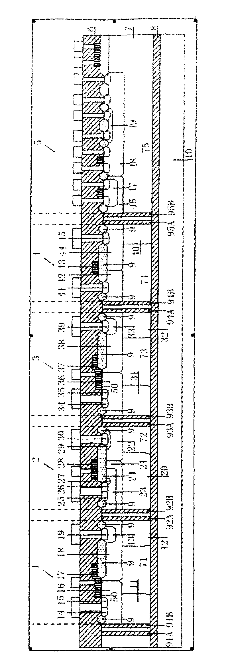
[0020] Below in conjunction with accompanying drawing, structure of the present invention is described in detail, as figure 1 As shown, a high and low voltage device for a plasma display driver chip includes a P-type substrate 10, a buried oxide layer 8 is arranged on the P-type substrate 10, and a high-voltage N-type lateral insulated gate double layer is arranged on the buried oxide layer 8. Pole type transistor 1, high-voltage P-type lateral double-diffused metal-oxide-semiconductor field-effect transistor 2, high-voltage N-type lateral double-diffused metal-oxide-semiconductor field-effect transistor 3, high-voltage diode 4 and low-voltage device 5, characterized in that the high-voltage N-type lateral The insulated gate bipolar transistor 1 is adjacent to the high-voltage P-type lateral double-diffused metal-oxide-semiconductor field-effect transistor 2, and the drain terminal of the high-voltage N-type lateral insulated-gate bipolar transistor 1 is connected to the high-v...

Embodiment 2

[0031] The preparation method of the high and low voltage device for the plasma display driver chip of the present invention is as follows:

[0032] The first step: take a P-type substrate 10 with an impurity concentration of 1.0e15cm-3, and pre-clean it as shown in Figure 2(a); prepare a buried oxide layer 8 on the P-type substrate 10 as shown in Figure 2(b ); then grow a P-type epitaxial layer 7 with an impurity concentration of 1e15cm-3 as shown in FIG. High voltage N well 12 of insulated gate bipolar transistor 1, high voltage N well 20 of high voltage P-type lateral double diffused metal oxide semiconductor field effect transistor 2, high voltage N well of high voltage N type lateral double diffused metal oxide semiconductor field effect transistor 3 The well 32 and the high-voltage N well 40 of the high-voltage diode 4, after a simple treatment of rapid thermal annealing, directly inject boron with a dose of 3e12cm-2 and high-temperature annealing to form a high-voltage ...


PUM


Abstract

The invention provides a high-low voltage device for a plasma display driving chip and a preparation method. The device comprises a high-voltage N-type lateral isolation gate bipolar type transistor, a high-voltage P-type lateral double diffused metal oxide semiconductor field effect transistor, a high-voltage N-type lateral double diffused metal oxide semiconductor field effect transistor, a high-voltage diode and a low-voltage device. The preparation method comprises the following steps of: making a buried oxide layer and depositing a P-type epitaxial layer on the P-type substrate; making a high-voltage N-well and a high-voltage P-well of the high-voltage device on the P-type epitaxial layer; then making P-type body areas of the high-voltage N-type lateral isolation gate bipolar type transistor and the high-voltage P-type lateral double diffused metal oxide semiconductor field effect transistor on the P-type epitaxial layer; and making all low-voltage wells on the P-type epitaxial layer. The chip structure in the invention has the advantages of low chip power consumption, small chip area and high reliability, and can be compatible with manufacture technology of a standard low-voltage complementary type metal oxide semiconductor field effect transistor.

Description

technical field [0001] The invention relates to a high-voltage and low-voltage device for a display driving chip and a preparation method thereof, and is especially suitable for a row addressing driver chip and a column addressing driver chip for a plasma display (Plasma Display Panel, PDP). Background technique [0002] The plasma display is controlled and driven by the row driver chip and the column driver chip to realize the display of the image. The internal circuit of the chip is composed of low-voltage logic control circuit and high-voltage output drive device, among which the high-voltage output drive device directly lights up and controls the PDP display. With the continuous improvement of the design level and process manufacturing level of the driver chip, the characteristics of low cost, high frequency, high reliability, and low power consumption have become the development direction of the display driver chip. The manufacturing process of low-voltage logic contro...

Claims


Application Information

Patent Timeline
Patent Type & Authority Applications(China)
IPC IPC(8): H01L27/06H01L21/82G09G3/28
Inventor 易扬波李海松王钦刘侠陈文高
Owner SUZHOU POWERON IC DESIGN
Why Eureka
Try Eureka