Multiple quantum well structure for photoelectric device

A multi-quantum well structure, optoelectronic device technology, applied in electrical components, semiconductor devices, circuits, etc., can solve problems such as difficulty in making breakthroughs in brightness, low probability of electron and hole capture, and reduced probability of radiation recombination. Internal quantum efficiency, improve antistatic performance, improve reverse voltage effect

Inactive Publication Date: 2010-05-26
EPILIGHT TECH +1
View PDF0 Cites 21 Cited by
  • Summary
  • Abstract
  • Description
  • Claims
  • Application Information

AI Technical Summary

Problems solved by technology

However, first of all, because the electron concentration of the n-GaN layer is generally several orders of magnitude higher than the hole concentration in the p-GaN layer, this will cause the light-emitting interface to be close to the p-layer. When the light-emitting interface is close to the p-layer, only 1 -The radiative transition of the two quantum wells contributes to the luminescence, and it is difficult to make a big breakthrough in brightness. At the same time, because the luminous interface is close to the p-layer, the quantum well farther away from the p-layer has a non-radiative transition due to the existence of the quenching center. The probability of increasing the Joule heat will increase, which will make it difficult to effectively improve the life of the device; secondly, due to the large gap between the concentration and mobility of holes and electrons, electrons are easier to transport to deeper layers than holes The quantum well active area of ​​the quantum well, and the excess electrons will eventually form an ineffective current because they cannot recombine with the holes, thereby reducing the current injection efficiency of the device; finally, due to the polarization effect in the gallium nitride-based light-emitting diode, the quantum well There is a strong polarized electric field in the medium, and the electrons and holes are separated by space, resulting in a significant reduction in the probability of radiative recombination. Therefore, people usually use a narrower quantum well structure to increase the radiative recombination probability of electron holes, but the narrower quantum well structure It will lead to lower capture probability of electrons and holes, reducing the efficiency of LED current injection

Method used


Image

  • Multiple quantum well structure for photoelectric device
  • Multiple quantum well structure for photoelectric device
  • Multiple quantum well structure for photoelectric device

Examples


Embodiment Construction

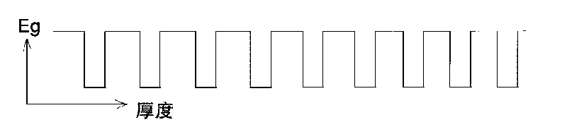
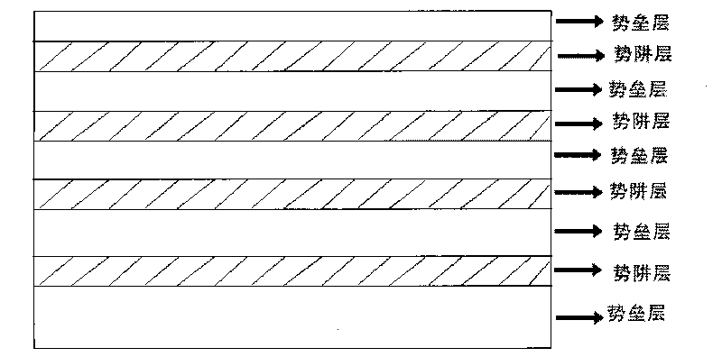
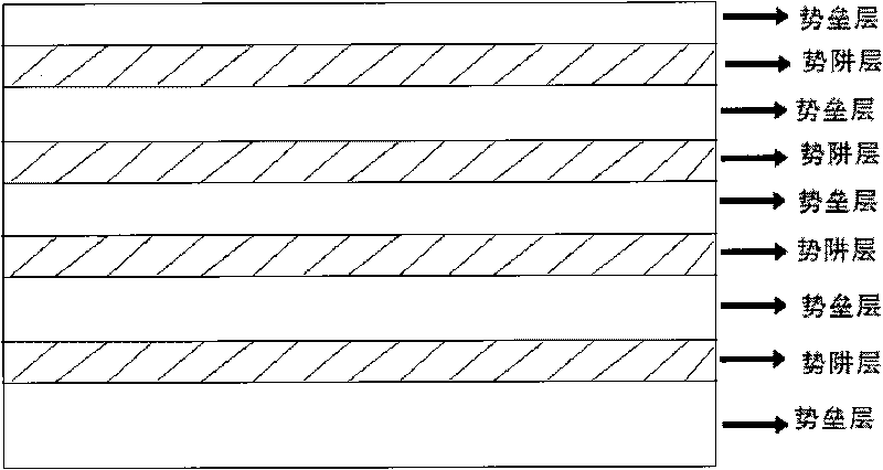
[0009] like figure 1 , figure 2 As shown, the present invention provides a multi-quantum well structure for optoelectronic devices, including n sequentially overlapping quantum well structures. The thickness of the barrier layer is greater than the thickness of the barrier layer close to the P-type semiconductor layer; the n is an integer greater than 2 and less than 20.

[0010] The thicknesses from the mth potential well layer to the nth potential barrier layer near the N-type semiconductor layer can be gradually reduced, and the m is an integer greater than 0 and less than n.

[0011] The potential well layers of the first m quantum wells close to the N-type semiconductor layer may have the same thickness, and the thicknesses of the m+1th to nth potential barrier layers become thinner successively, and the m is an integer greater than 0 and less than n.

[0012] The thickness of the potential well layers of the first m quantum wells close to the N-type semiconductor laye...


PUM


Abstract

The invention discloses a multiple quantum well structure for a photoelectric device, which comprises n quantum well structures overlapped sequentially. The photoelectric device comprises an N-type semiconductor layer and a P-type semiconductor layer, and is characterized in that the thickness of the barrier layer close to the N-type semiconductor layer is larger than the thickness of the barrier layer close to the P-type semiconductor layer; and n is an integer which is larger than 2 and less than 20. The invention can improve the internal quantum efficiency, and because the barrier layer close to the N layer is wider, the invention can compel holes to move near to the N layer, thereby increasing the number of luminous quantum wells and improving the luminous efficiency of the quantum wells and the brightness. The invention can increase the backward voltage and improve the antistatic property, and because the barrier layer close to the N layer is thicker than the barrier layer close to the P layer, a PN junction is widened when the backward voltage is applied.

Description

technical field [0001] The invention relates to a structure used in a photoelectric device, in particular to a multi-quantum well structure used in a photoelectric device. Background technique [0002] Light-emitting diodes (LEDs) semiconductor light-emitting diodes use electrons and holes to travel from n-type doped regions and p-type doped regions to the active region for recombination to generate radiative transitions and emit light. However, first of all, because the electron concentration of the n-GaN layer is generally several orders of magnitude higher than the hole concentration in the p-GaN layer, this will cause the light-emitting interface to be close to the p-layer. When the light-emitting interface is close to the p-layer, only 1 -The radiative transition of the two quantum wells contributes to the luminescence, and it is difficult to make a big breakthrough in brightness. At the same time, because the luminous interface is close to the p-layer, the quantum well...

Claims


Application Information

Patent Timeline
Patent Type & Authority Applications(China)
IPC IPC(8): H01L33/06H01L31/0352
Inventor 李淼颜建锋周健华顾拓郝茂盛
Owner EPILIGHT TECH
Why Eureka
Try Eureka