Punching die of long-slotted holes of integrated circuit boards

A technology for integrated circuit boards and long slot holes, applied in the field of punching dies, to achieve the effects of reducing the cost of use, wide application range, and ensuring processing accuracy

Inactive Publication Date: 2010-06-16
苏州均华精密机械有限公司
View PDF0 Cites 7 Cited by
  • Summary
  • Abstract
  • Description
  • Claims
  • Application Information

AI Technical Summary

Problems solved by technology

[0004] The invention provides a punching die for long slot holes of integrated circuit boards, which aims to solve the problems existing in the processing of long slot holes of integrated circuit boards by high-speed numerical control milling machines, improve processing efficiency and quality, reduce processing costs, and adapt to large-scale The need for mass production

Method used


Image

  • Punching die of long-slotted holes of integrated circuit boards
  • Punching die of long-slotted holes of integrated circuit boards
  • Punching die of long-slotted holes of integrated circuit boards

Examples


Embodiment

[0030] Example: a long slot hole punching die for an integrated circuit board

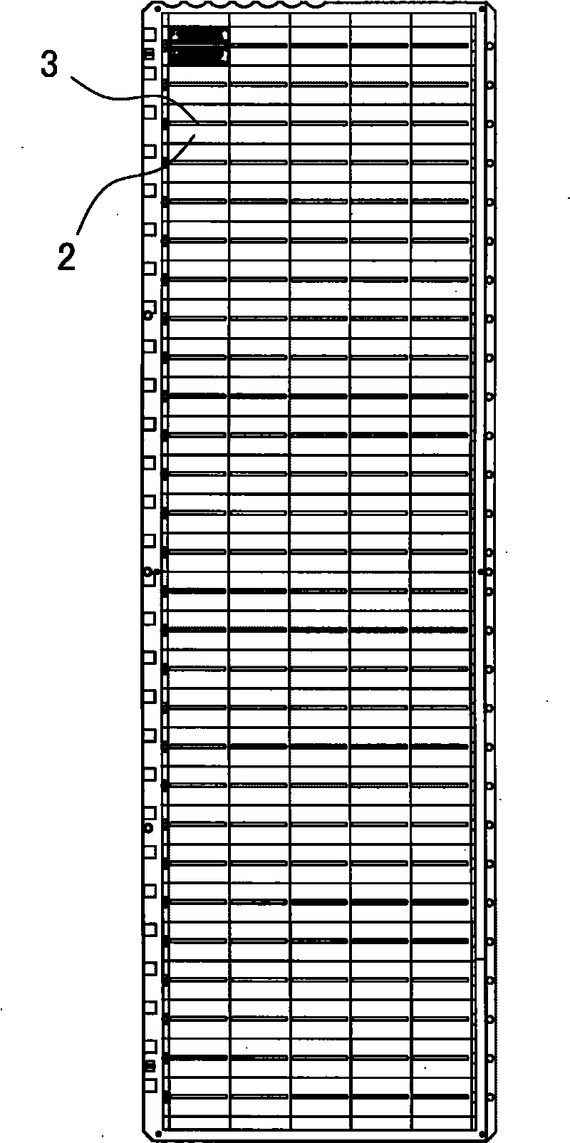
[0031] This embodiment requires processing objects, see image 3 shown, image 3 It is a schematic diagram of the whole board composed of multiple integrated circuit boards and 2 units. There is a long slot 3 in the center of each integrated circuit board 2 . The present invention utilizes a punching die with long slot holes for one-time punching and forming. The overall structure of the long slot punching die is described below.

[0032] like Figure 4 to Figure 8 As shown in the figure, the mold is a sub-mother mold split structure, and the entire mold is mainly composed of the upper mold 8 of the master mold (see Figure 4 ), master die lower die 9 (see Figure 5 ), sub-die upper die 11 (see Image 6 ), sub-die lower die 16 (see Figure 7 )composition. The upper mold 11 of the child mold is installed on the upper mold 8 of the master mold, and the lower mold 16 of the child mold is inst...


PUM


Abstract

The invention relates to a punching die of long-slotted holes of integrated circuit boards. The punching die comprises a male die and a female die and is characterized in that the male die consists of a set of punching tools arranged corresponding to the positions of long-slotted holes; each punching tool is flake-shaped; the shape and the size of the cross section of each punching tool are identical to those of the long-slotted holes, while the punching head is dovetail-shaped; the female die consists of a set of punching blades arranged corresponding to the punching tools; and the shape and the size of the punching blades are identical to those of the long-slotted holes. The punching die solves the problems of the prior art which adopts a high-speed numerical control milling machine to process the long-slotted holes of the integrated circuit boards and improves processing efficiency and quality to reduce processing cost. The punching die is suitable to process long-slotted holes on a packaging substrate of a semiconductor chip, and the substrate comprises a matrix-type ball-type arrangement integrated circuit board (BGA), a ball-type arrangement composite chip integrated circuit board (BOC) and a plastic surface adhesion composite chip integrated circuit board (PVC).

Description

technical field [0001] The invention relates to a punching die, in particular to a punching die for punching long slot holes of an integrated circuit board. The integrated circuit board refers to a substrate containing a printed circuit used in the packaging of semiconductor chips. Such substrates include matrix ball array (BGA), ball array composite chip (BOC) and plastic surface mount composite chip (PVC). Background technique [0002] With the development of integrated circuit technology, most integrated circuit chips nowadays use surface mount packaging technology (Surface Mounted Devices for short SMD). In this chip package structure, the semiconductor wafer is seated on an integrated circuit board. The integrated circuit board not only acts as a package substrate, which plays a role of positioning and support, but also acts as a single-layer or multi-layer printed circuit board, which plays an electrical connection role, that is, the integrated circuit board can be e...

Claims


Application Information

Patent Timeline
IPC IPC(8): B21D28/34B26F1/14
Inventor 林先传龚利华
Owner 苏州均华精密机械有限公司
Why Eureka
Try Eureka