Cadmium telluride in-situ passivation method of mercury cadmium telluride infrared focal plane chip

An infrared focal plane, mercury cadmium telluride technology, applied in sustainable manufacturing/processing, electrical components, climate sustainability, etc., can solve the problem of affecting the process stability of the device, loss of part passivation of the mercury cadmium telluride infrared focal plane detection chip performance, mercury cadmium telluride detection chip surface contamination and other issues, to achieve the effect of good passivation effect, high stability and convenient operation

Active Publication Date: 2010-06-16
SHANGHAI INST OF TECHNICAL PHYSICS - CHINESE ACAD OF SCI
View PDF0 Cites 9 Cited by
  • Summary
  • Abstract
  • Description
  • Claims
  • Application Information

AI Technical Summary

Problems solved by technology

However, during the entire chip manufacturing process, the fresh surface of the HgCdTe infrared detection chip will be exposed to the air for a short time or a long time before the growth of the CdTe passivation film, thus causing the surface of the HgCdTe detection chip to be oxidized and stained. dirty
This will lose the passivation performance of the HgCdTe infrared focal plane detection chip and affect the stability of the device process

Method used


Image

  • Cadmium telluride in-situ passivation method of mercury cadmium telluride infrared focal plane chip
  • Cadmium telluride in-situ passivation method of mercury cadmium telluride infrared focal plane chip
  • Cadmium telluride in-situ passivation method of mercury cadmium telluride infrared focal plane chip

Examples


Embodiment Construction

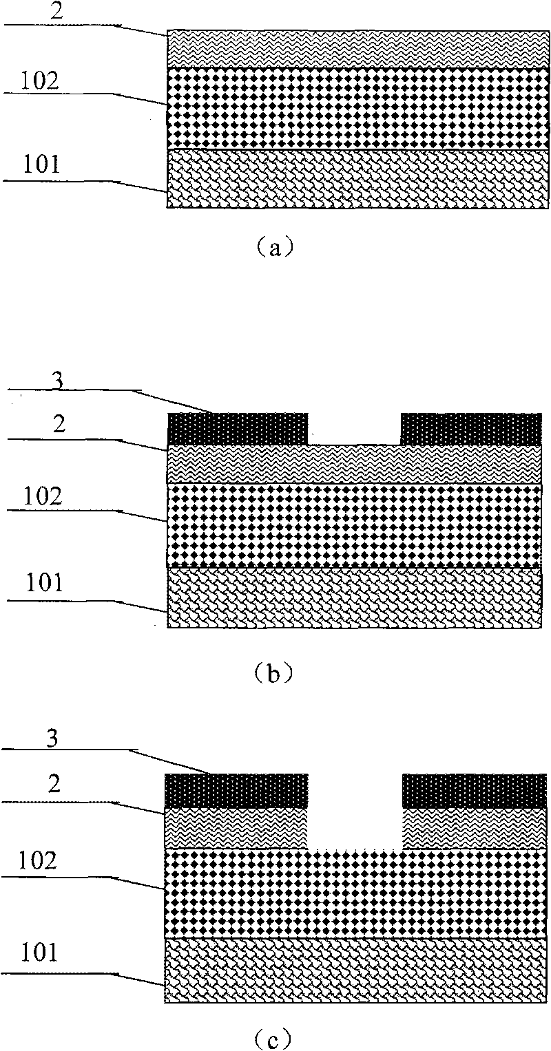
[0019] Below in conjunction with accompanying drawing, the specific embodiment of the present invention is described in further detail:

[0020] A. Using molecular beam epitaxy, at the end of the growth of the mercury cadmium telluride infrared detection material 1, a layer of cadmium telluride film 2 is grown in situ on the surface of the mercury cadmium telluride film 102, and the film thickness is

[0021] B. Using traditional photolithography technology, on the surface of the HgCdTe infrared focal plane detection chip, a photoresist masking film pattern 3 for limiting the ion implantation area is made. The thickness of the masking film is 1-3 μm, and the ion implantation area defined by the masking film pattern is Square array, the square side length is 20μm.

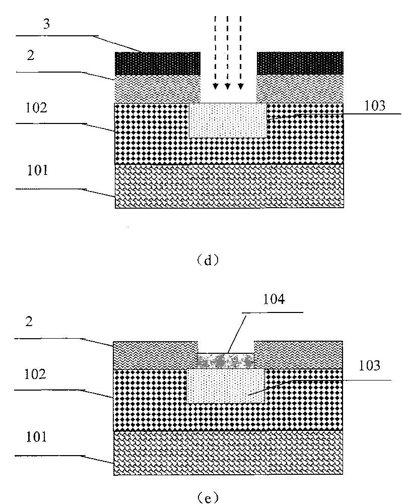
[0022] C. Utilize the wet chemical etching method to etch away the cadmium telluride thin film in situ in the ion implantation area limited by the pattern of the photoresist masking film. The etching solution used...


PUM


Abstract

The invention discloses a cadmium telluride in-situ passivation method of a mercury cadmium telluride (HgCdTe) infrared focal plane chip, which relates to a manufacturing process technology of a photoelectric detector. The invention adopts the technical scheme that the cadmium telluride in-situ passivation method comprises the following steps of: at the end point of a mercury cadmium telluride infrared detection material grown by molecular beam epitaxy, firstly in situ growing a layer of cadmium telluride film on the surface of an HgCdTe film and carrying out nondestructive cadmium telluride in-situ passivation for the cadmium telluride film at a region to be passivated in the preparation process of an HgCdTe infrared detection chip, thereby effectively solving the problems of detection performance loss and low process stability of a mercury cadmium telluride (HgCdTe) infrared focal plane detection chip caused by a conventional cadmium telluride passivation method. The method has the characteristics of simple process, convenient operation, high stability and good passivation effect.

Description

technical field [0001] The invention relates to a manufacturing process technology of a photodetector device, in particular to a cadmium telluride in-situ passivation method for a mercury cadmium telluride (HgCdTe) infrared focal plane detector detection chip. Background technique [0002] Infrared focal plane array device is an advanced imaging sensor with both infrared information acquisition and information processing functions. There are important and extensive applications in military and civilian fields. Due to its irreplaceable status and role, major industrial countries in the world have listed HgCdTe infrared focal plane array device manufacturing technology as a high-tech project for key development. [0003] Driven by the advanced infrared application system, infrared detection technology has entered an important development stage of the third generation infrared focal plane detector characterized by large area array, miniaturization and multicolor, see S.Horn, P...

Claims


Application Information

Patent Timeline
Patent Type & Authority Applications(China)
IPC IPC(8): H01L31/18
CPCY02P70/50
Inventor 叶振华黄建胡伟达尹文婷林春陈路廖清君胡晓宁丁瑞军何力
Owner SHANGHAI INST OF TECHNICAL PHYSICS - CHINESE ACAD OF SCI
Why Eureka
Try Eureka