Thermal interface material

A thermal interface material and metal technology, applied in the direction of heat exchange materials, chemical instruments and methods, etc., can solve the problems of poor contact, increased interface thermal resistance, large interface thermal resistance, etc., and achieve tight contact and small contact thermal resistance. , the effect of reducing thermal resistance

Inactive Publication Date: 2010-06-23
SOUTHEAST UNIV
View PDF2 Cites 5 Cited by
  • Summary
  • Abstract
  • Description
  • Claims
  • Application Information

AI Technical Summary

Problems solved by technology

However, the contact between the end of the existing carbon nanotubes and the heat source and heat sink is poor, usually van der Waals force contact, so the interface thermal resistance is relatively large
The length of the carbon nanotube array is different, and the contact area between the actual carbon nanotubes and the heat sink or heat source is small, resulting in a further increase in the interface thermal resistance

Method used


Image

  • Thermal interface material
  • Thermal interface material
  • Thermal interface material

Examples


Embodiment 1

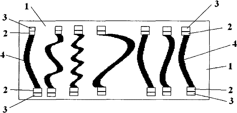
[0023] A thermal interface material, comprising a low-melting point metal and a carbon nanotube array formed by directional arrangement of carbon nanotubes, the preparation method of the carbon nanotube array is described below, wherein the average length of the carbon nanotubes in the carbon nanotube array is 1-150 Micron (before bending), for example can be selected as: 1 micron, 10 micron, 25 micron, 40 micron, 50 micron, 75 micron, 90 micron, 100 micron, 115 micron, 120 micron, 150 micron, described low melting point metal is Sn-lead alloys, tin-bismuth alloys, tin-silver-copper alloys, tin-zinc alloys and other alloys with a melting point below 400 degrees Celsius. Carbon nanotubes are single-walled or multi-walled carbon nanotubes. Multi-walled carbon nanotubes refer to carbon nanotubes with more than 2 walls. Nanotubes can be 3, 5, 6, 8 walls, etc. The volume occupied by carbon nanotubes accounts for 1-50% of the total volume of carbon nanotube arrays, usually 5-20%, for...

Embodiment 2

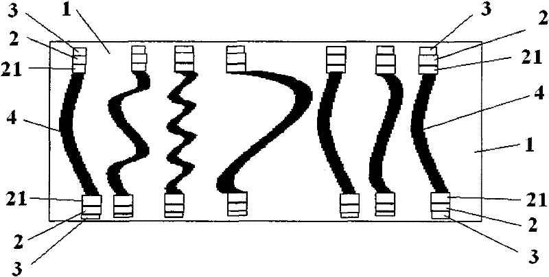
[0028] The preparation method of the thermal interface material described in Example 1 includes the following steps. The first step is to prepare a carbon nanotube array on the growth sheet. The carbon nanotubes used are the same as in Example 1. The preparation method of the carbon nanotubes is described below. The second The first step is to deposit a metal wetting layer and a metal transition layer on both ends of the carbon nanotube: deposit a metal wetting layer on the free end surface (necessary plasma cleaning before this) and a metal transition layer, such as: Ti / Cu / Au, or Ti / Ni / Au, or W / Cu / Au, or W / Ta / Au, or Al / Ni / Au, or Cr / Cu / Au, or Ti / W / Au, and then transfer the carbon nanotube array to another On the substrate, the same metal wetting layer and metal transition layer are deposited on the other end face of the carbon nanotube array. The deposition method is magnetron sputtering, and the deposition rate is 80-120 Angstroms / min. Choose to use the aforementioned micro...

Embodiment 3

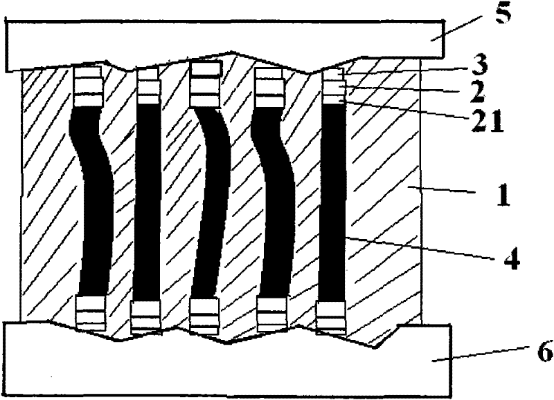
[0030] A thermal interface material, including low-melting-point metal SAC305 and a carbon nanotube array formed by directional arrangement of carbon nanotubes, the preparation method of the carbon nanotube array is as follows, wherein the average length of the carbon nanotubes in the carbon nanotube array is 75 microns , the carbon nanotubes are aligned in parallel, the carbon nanotubes are multi-walled carbon nanotubes, and the volume occupied by the carbon nanotubes accounts for 4.5% of the total volume of the carbon nanotube arrays. The carbon nanotube array is elastically bent in the solidified low-melting point metal, and the two ends of the carbon nanotubes are provided with a metal wetting layer, and the metal wetting layer is titanium. It can also be seen from the SEM topography in the attached drawing Wetting well with the carbon nanotubes can significantly reduce the contact thermal resistance between the low-melting point metal and the carbon nanotubes, and the thic...


PUM

PropertyMeasurementUnit
Thicknessaaaaaaaaaa
Average lengthaaaaaaaaaa
Thicknessaaaaaaaaaa

Abstract

The invention discloses a thermal interface material which comprises low-melting point metal and a carbon nanometer tube array formed by directionally arranging carbon nanometer tubes, wherein the carbon nanometer tube array is elastically bent in the low-melting point metal; a metal wetting layer is arranged at two end parts of each carbon nanometer tube; and a metal transition layer is arranged between the metal wetting layer and the low-melting point metal. In the invention, a better transitional crystal structure is formed between the metal wetting layer and each carbon nanometer tube through forming metallic carbide between the metal wetting layer and each carbon nanometer tube in a reaction manner. Compared with an interface between the metal wetting layer in a wetting state and each carbon nanometer tube, the dispersion of a phonon, an electron and other hot carriers can be further reduced, and thermal contact resistance between each carbon nanometer tube and a hot source can be further reduced. The carbide with the crystal structure has better thermal conductivity.

Description

technical field [0001] The invention relates to a preparation method of a microelectronic material, in particular to a thermal interface material. Background technique [0002] When the integrated circuit chip is working in a very small space, it will generate a lot of heat. Therefore, the heat generated must be dissipated in an appropriate way to prevent the integrated circuit chip from overheating and causing operational errors and even serious problems. cause hardware circuit damage. Therefore, the heat dissipation problem in the package becomes more and more critical. [0003] In the prior art, heat sinks are usually used to manage heat sources such as high-power components, such as chips. Therefore, the contact interface between the heat sink and the heat source becomes the heat dissipation channel of the heat source. However, since the respective surfaces of the heat source and the heat dissipation device have relatively large roughness, their actual microscopic con...

Claims


Application Information

Patent Timeline
IPC IPC(8): C09K5/06
Inventor 尚金堂徐超张迪陈波寅黄庆安
Owner SOUTHEAST UNIV
Why Eureka
Try Eureka