Light-emitting device and manufacturing method thereof
A light-emitting device, photoluminescence technology, applied in the direction of semiconductor devices, electrical components, circuits, etc., can solve the problems of uneven phosphor powder, aging yellowing, large scattering of phosphor powder particles, etc., to avoid process instability and avoid The effect of aging and yellowing
- Summary
- Abstract
- Description
- Claims
- Application Information
AI Technical Summary
Problems solved by technology
Method used
Image
Examples
Embodiment approach 1
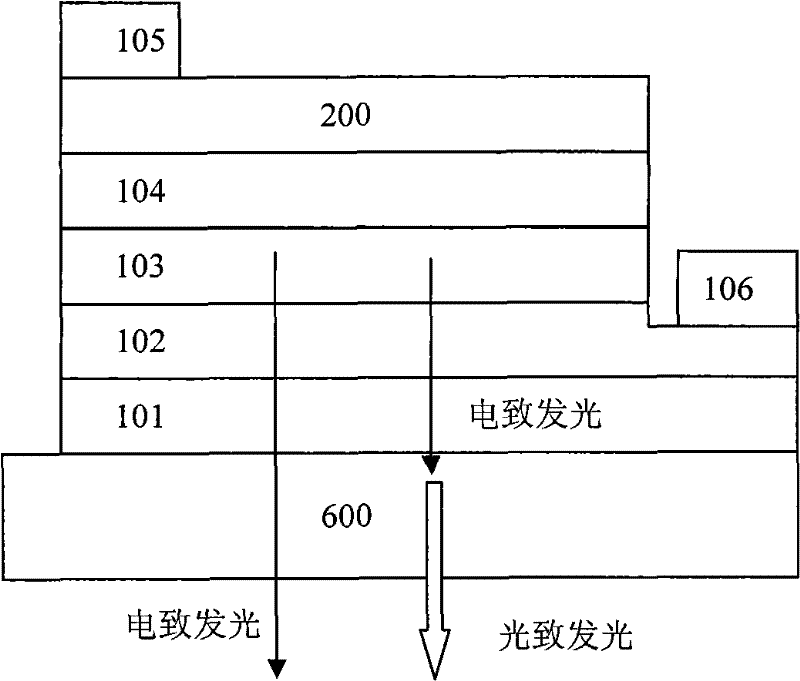
[0029] figure 2 A schematic structural view of a light emitting device according to an embodiment of the present invention is shown. The light-emitting device includes: a light-emitting diode, a reflective layer 200 and a crystal substrate 600 with photoluminescent function. Wherein the light-emitting diode includes: the crystal growth transition layer 101 of the light-emitting diode, the electron-type conductive layer 102 of the light-emitting diode, the light-emitting layer 103 of the inorganic light-emitting diode, the hole-type conductive layer 104 of the light-emitting diode, and the hole-type conductive electrode 105 of the light-emitting diode , The electronic conductive electrode 106 of the light emitting diode.
[0030] figure 2 The working principle of the light-emitting device shown is as follows: the light-emitting layer 103 of the light-emitting diode emits light with a wavelength range from ultraviolet to blue-green (the wavelength range of light can be selec...
Embodiment approach 2
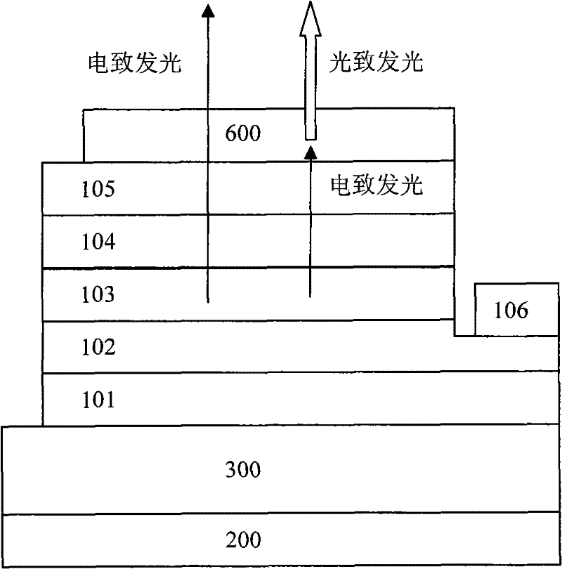
[0036] image 3 A schematic structural view of a light emitting device according to another embodiment of the present invention is shown. image 3 The light-emitting device shown includes: a light-emitting diode, a substrate 300 of the light-emitting diode, a reflective layer 200, and a crystal substrate 600 capable of emitting light. Wherein the light-emitting diode comprises: the crystal growth transition layer 101 of the light-emitting diode, the electron-type conductive layer 102 of the light-emitting diode, the light-emitting layer 103 of the light-emitting diode, the hole-type conductive layer 104 of the light-emitting diode, the hole-type conductive electrode 105 of the light-emitting diode, Electronically conductive electrode 106 of the LED.
[0037] In this embodiment, each semiconductor layer of the light-emitting diode (including the crystal growth transition layer 101 of the light-emitting diode, the electron-type conductive layer 102 of the light-emitting diode, ...
PUM
 Abstract
Description
Claims
Application Information
 - R&D
- Intellectual Property
- Life Sciences
- Materials
- Tech Scout
- Unparalleled Data Quality
- Higher Quality Content
- 60% Fewer Hallucinations
Browse by: Latest US Patents, China's latest patents, Technical Efficacy Thesaurus, Application Domain, Technology Topic, Popular Technical Reports.
© 2025 PatSnap. All rights reserved.Legal|Privacy policy|Modern Slavery Act Transparency Statement|Sitemap|About US| Contact US: help@patsnap.com


