PCB (Printed Circuit Board) processing method

A processing method and a technology for a resist layer, which are applied in the formation of electrical connection of printed components, electrical components, and printed circuit manufacturing, etc., can solve the problems of limited dry film sealing ability, poor dry film adhesion, and easy shovel of resin. , to achieve the effect of reducing the risk of scrapping, improving the process capacity and reducing the cost of scrapping

Active Publication Date: 2010-07-07
SHENNAN CIRCUITS
View PDF0 Cites 6 Cited by
  • Summary
  • Abstract
  • Description
  • Claims
  • Application Information

AI Technical Summary

Problems solved by technology

[0005] 1) The sealing ability of the dry film is limited. When there are large metallized holes and grooves or side metallization, this process cannot be processed;
[0006] 2) The resin is easy to shovel, and the residual resin will cause poor adhesion of the dry film and high scrap cost;
[0007] 3) The dry film is easily scratched and the cost of scrapping is high

Method used


Image

  • PCB (Printed Circuit Board) processing method
  • PCB (Printed Circuit Board) processing method
  • PCB (Printed Circuit Board) processing method

Examples


Embodiment Construction

[0028] In order to describe the technical content, structural features, achieved goals and effects of the present invention in detail, the following will be described in detail in conjunction with the embodiments and accompanying drawings.

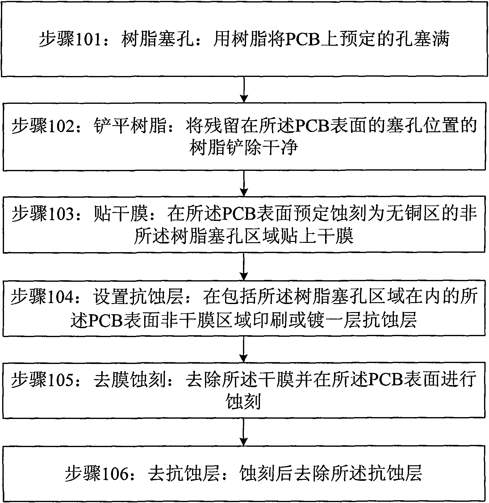
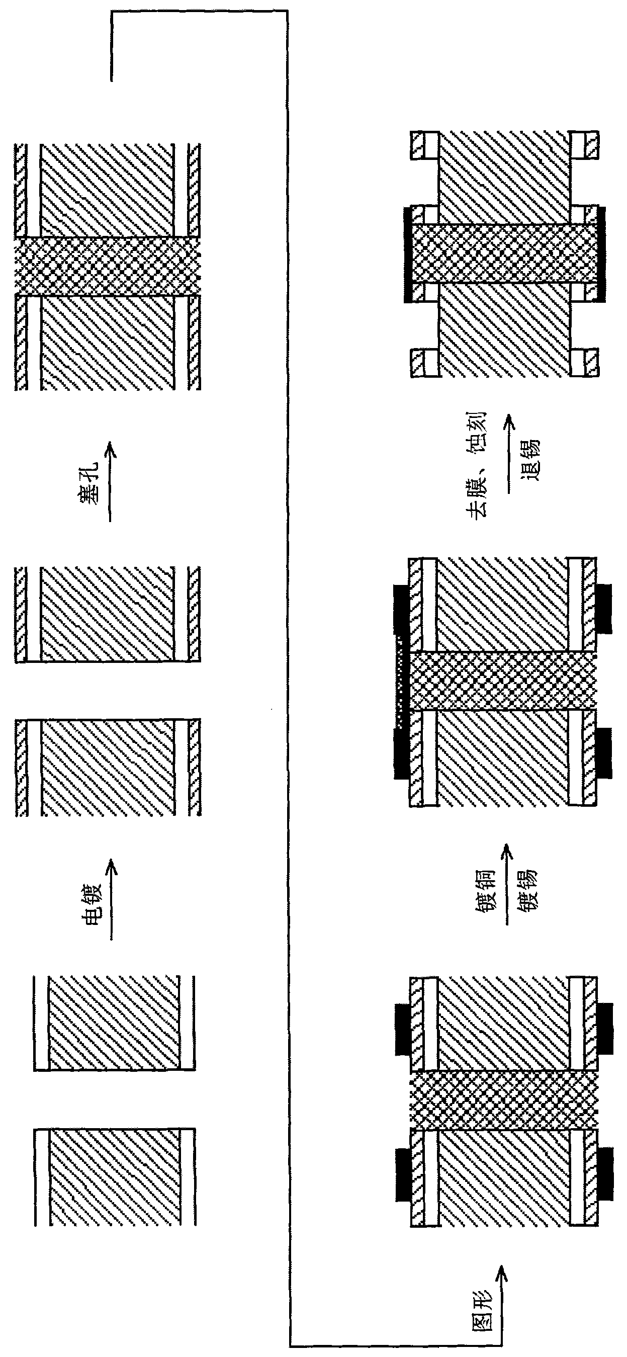
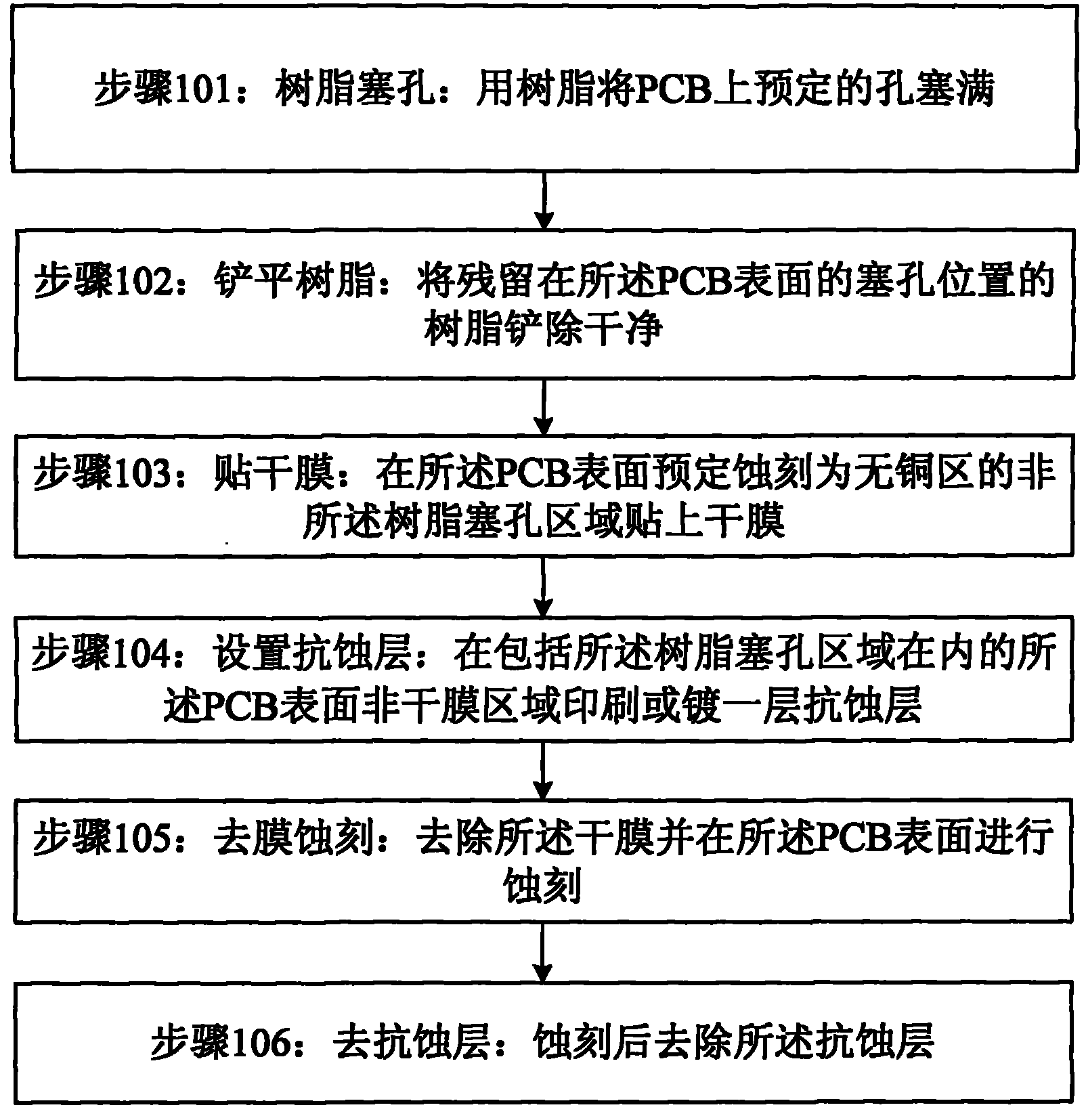
[0029] see figure 1 as well as figure 2 , the PCB processing method embodiment of the present invention mainly comprises the following steps:

[0030] Step 101: Resin plugging holes: filling predetermined holes on the PCB with resin;

[0031] Step 102: leveling the resin: removing the resin remaining at the plug holes on the surface of the PCB;

[0032] Step 103: Sticking a dry film: sticking a dry film on the area of ​​the PCB surface that is not scheduled to be etched as a copper-free area, but not the resin plug hole area;

[0033] That is, paste a dry film on the surface of the PCB that will be etched as a copper-free area;

[0034] Step 104: setting a resist layer: printing or plating a resist layer on the non-dry film area of ​​...


PUM


Abstract

The invention discloses a PCB (Printed Circuit Board) processing method which comprises the following steps of: resin hole cramming: cramming preset holes on a PCB by using resin; resin leveling: shoveling resin left at the positions of the crammed holes on the surface of the PCB completely; drying film pasting: pasting a dry film on a non-resin hole cramming area preset to be etched into a copper-free area on the surface of the PCB; anti-corrosion layer arrangement: printing or plating an anti-corrosion layer on a non dry film area on the surface of the PCB, which comprises the resin hole cramming areas; film removing and etching: removing the dry film and etching on the surface of the PCB; and anti-corrosion layer removing: removing the anti-corrosion layer after etching. The invention has good adaptability to the resin hole cramming process and can greatly reduce the scrap cost.

Description

technical field [0001] The invention relates to a processing method, in particular to a PCB processing method. Background technique [0002] The PCB industry is currently in the era of HDI high-density connection technology, and the trend of line width and line spacing is becoming smaller and denser. As a result, different types of PCB structures have emerged, such as Via on Pad, Stack Via, etc. Under this premise, the buried holes in the inner layer are usually required to be completely filled and ground flat to increase the wiring area of ​​the outer layer. This process is called "plug hole" in the industry. [0003] In the outer layer plugging process, the via holes of PCB boards used for packaging are required to be plugged with oil or resin to prevent other functional hazards caused by tin hidden in the holes. Now multi-layer boards are required to plug holes with solder-proof green paint ; Blind and buried holes in the inner layer also require plug hole processing. ...

Claims


Application Information

Patent Timeline
Patent Type & Authority Applications(China)
IPC IPC(8): H05K3/00H05K3/42
Inventor 魏厚斌李雷罗斌秦运杰
Owner SHENNAN CIRCUITS
Why Eureka
Try Eureka