A kind of mems microbridge structure contact hole preparation method

A technology of micro-bridge structure and contact hole, which is applied in the direction of micro-structure technology, micro-structure devices, manufacturing micro-structure devices, etc., can solve the problems of difficult precise control of alignment accuracy, high R&D and production costs, and achieve improved alignment accuracy and Effect of Process Window, Improved Performance, and Avoided Alignment Errors

Active Publication Date: 2015-08-12
SHANGHAI INTEGRATED CIRCUIT RES & DEV CENT +1
View PDF5 Cites 0 Cited by
  • Summary
  • Abstract
  • Description
  • Claims
  • Application Information

AI Technical Summary

Problems solved by technology

In this preparation process, the patterning process of the support hole and the contact hole requires two steps of photolithography and two photolithography masks, and the development and production costs are high. At the same time, the alignment accuracy is difficult to control accurately

Method used


Image

  • A kind of mems microbridge structure contact hole preparation method
  • A kind of mems microbridge structure contact hole preparation method
  • A kind of mems microbridge structure contact hole preparation method

Examples


Embodiment Construction

[0028] In order to make the object, technical solution and advantages of the present invention clearer, the present invention will be further described in detail below in conjunction with the accompanying drawings.

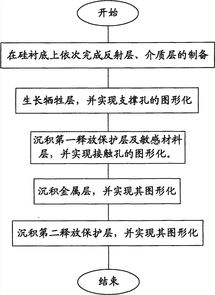
[0029] figure 1 The flow chart of the first specific embodiment of the method for preparing the contact hole of the MEMS microbridge structure provided by the present invention.

[0030] Such as figure 1 As shown, the MEMS microbridge structure contact hole preparation method provided in this specific embodiment includes the following steps:

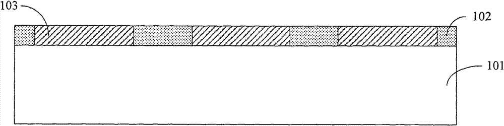
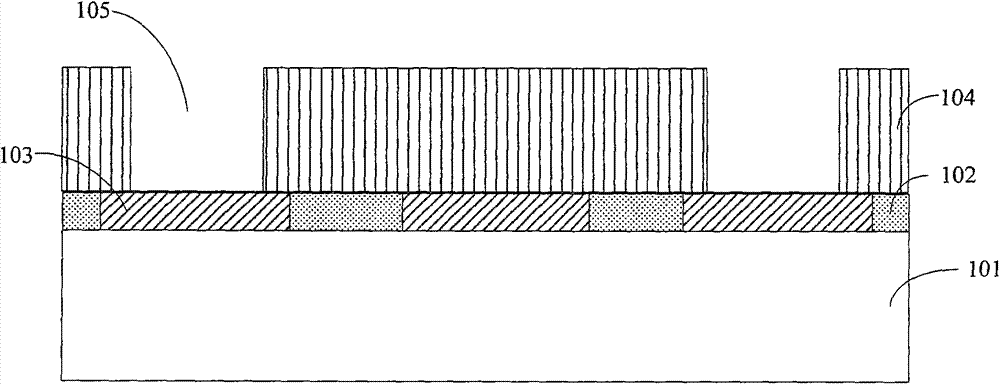
[0031] In step one, the reflection layer 103 and the dielectric layer 102 are sequentially prepared on the silicon substrate 101 .

[0032] In this step, the reflective layer 103 used as the connecting electrode is first grown, patterned by photolithography, and then the dielectric layer 102 is deposited and polished by chemical mechanical polishing (CMP) until the surface of the reflective layer 103 is exposed. The mater...


PUM


Abstract

The invention discloses an MEMS microbridge structure contact hole preparation method, which comprises the completion of a reflecting layer, a dielectric layer, a sacrificing layer, a release protecting and supporting layer and a metal layer on a semiconductor silicon substrate subsequently, and deposition and imaging of a sensitive material layer formed on a metal electrode surface and the release protecting and supporting layer which is not covered by the metal electrode. In the MEMS microbridge structure contact hole preparation method provided by the invention, photoetching exposure is achieved on supporting holes and contact hole graphs inside the supporting holes by using the same photoetching mark, thus greatly lowering the production and research and development cost of products, improving processing window, and enhancing MEMS property, yield and reliability correspondingly.

Description

technical field [0001] The invention relates to a MEMS manufacturing process, in particular to the preparation of a MEMS micro-bridge structure, and belongs to the technical field of semiconductors. Background technique [0002] Micro-Electro-Mechanica System (MEMS) technology has many advantages such as small size, executable, integrated, good process compatibility, and low cost, so it has begun to be widely used in many fields. [0003] The MEMS micro-bridge structure is a very widely used structure in the MEMS field. It uses a sacrificial layer release process to form a bridge structure, which can be widely used in detectors, sensors and other products. In the MEMS micro-bridge structure, the contact hole plays a very critical role in the electrical connection of the micro-bridge structure in some pillar-free connections, so the basic space is very critical to the entire detector. In the prior art, when preparing the contact holes of the MEMS microbridge structure, the s...

Claims


Application Information

Patent Timeline
Patent Type & Authority Patents(China)
IPC IPC(8): B81C1/00
Inventor 康晓旭姜利军蒋宾赵宇航庞惠民
Owner SHANGHAI INTEGRATED CIRCUIT RES & DEV CENT
Why Eureka
Try Eureka