Preparation method of graphene MOS transistor

A MOS transistor and graphene technology, applied in semiconductor/solid-state device manufacturing, semiconductor devices, electrical components, etc., can solve problems such as excessive off-current, reduce contact resistance, expand band gap, and reduce gate The effect of leakage current

Inactive Publication Date: 2010-07-21
FUDAN UNIV
View PDF3 Cites 38 Cited by
  • Summary
  • Abstract
  • Description
  • Claims
  • Application Information

AI Technical Summary

Problems solved by technology

[0005] The purpose of the present invention is to propose a novel graphene MOS transistor, whic

Method used


Image

  • Preparation method of graphene MOS transistor
  • Preparation method of graphene MOS transistor
  • Preparation method of graphene MOS transistor

Examples


Embodiment Construction

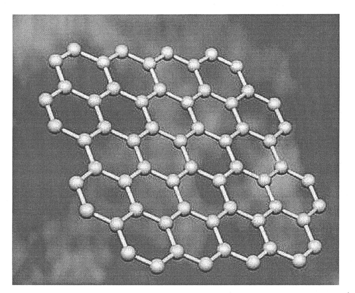
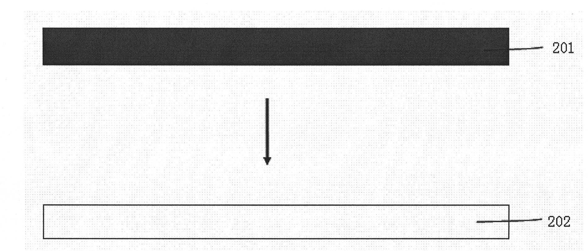
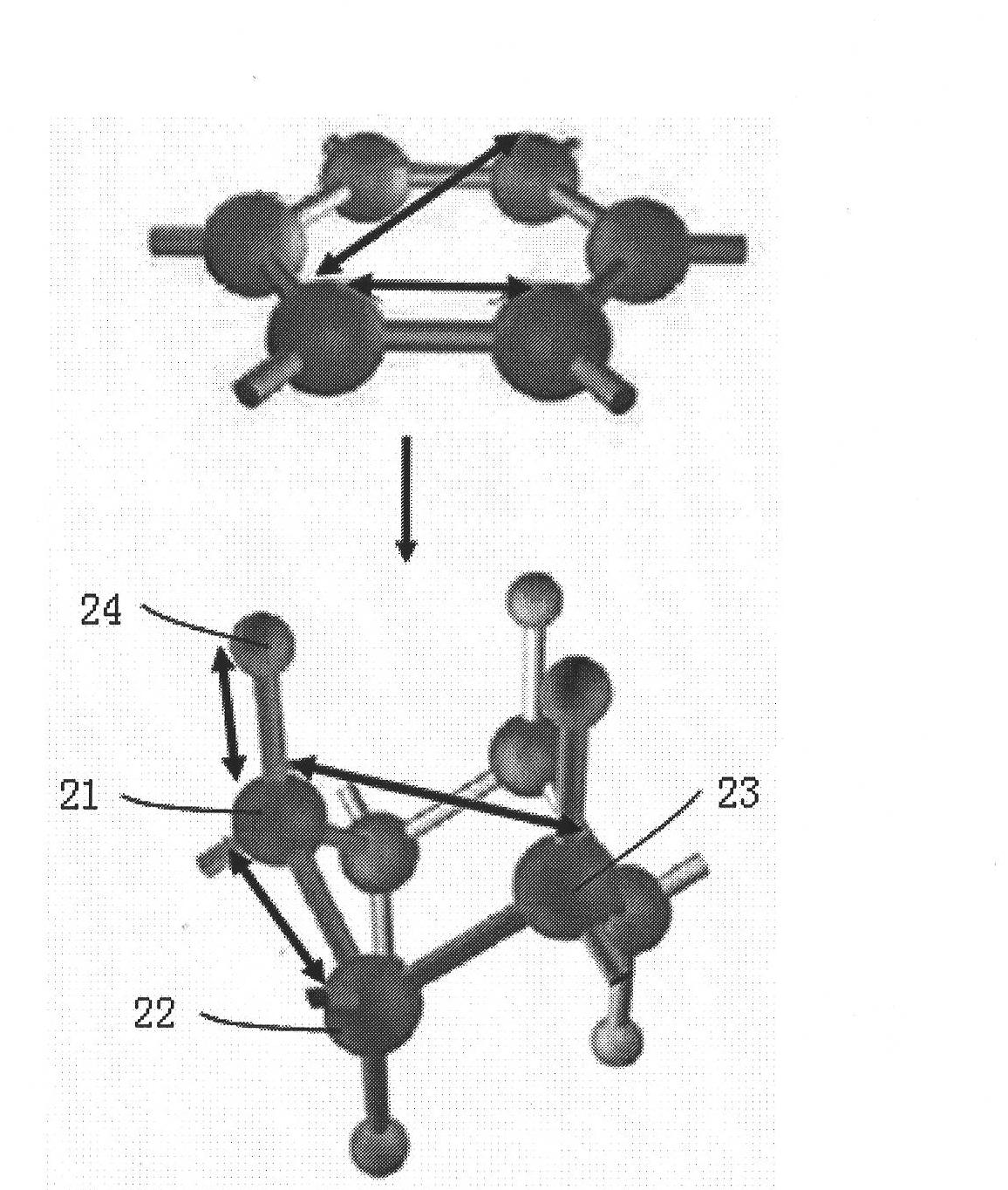
[0020] An exemplary embodiment of the present invention will be described in detail below with reference to the accompanying drawings. In the drawings, the thicknesses of layers and regions are enlarged or reduced for convenience of description, and the shown sizes do not represent actual sizes. Although these figures do not fully reflect the actual size of the device, they still completely reflect the mutual positions between the regions and the constituent structures, especially the upper-lower and adjacent relationships between the constituent structures. The referenced figures are schematic illustrations of idealized embodiments of the invention, and the illustrated embodiments of the invention should not be construed as limited to the particular shapes of regions illustrated in the figures but are to include resulting shapes, such as manufacturing-induced deviations. For example, the curves obtained by etching are usually curved or rounded, but in the embodiment of the pr...


PUM


Abstract

The invention belongs to the technical field of semiconductor devices and particularly discloses a preparation method of a graphene MOS transistor, which is as follows: firstly intrinsic grapheme is processed through hydrogen plasma to obtain hydrogenated graphene, and then the large pi bonds of the graphene are destructed through the method of atomic layer metallic oxide deposition. In this way, the forbidden gap of the graphene can be effectively expanded and the gate leakage current in the graphene MOS transistor can be reduced. Meanwhile, the graphene with no metallic oxide deposition can maintain the semimetal property to be used as the source electrode and the drain electrode of the graphene MOS transistor, thus reducing the contact resistance between the source electrode and the channel. The preparation method is compatible with the existing CMOS technique and makes large grapheme-based integrated circuits possible.

Description

technical field [0001] The invention belongs to the technical field of semiconductor devices, and in particular relates to a MOS transistor and a preparation method thereof, in particular to a method of using graphene to prepare a high-speed nanometer MOS transistor with a source and a drain, and belongs to the field of semiconductor devices. Background technique [0002] Graphene is a single-layer carbon atom film exfoliated from graphite materials. On a two-dimensional plane, each carbon atom is connected with sp2 hybrid orbitals, that is, each carbon atom is connected to the three nearest neighbors. Three σ bonds are formed between carbon atoms, and the remaining p electron orbit is perpendicular to the graphene plane, forming π bonds with surrounding atoms, and the carbon atoms form a regular hexagonal planar honeycomb structure, so that only Two atoms with different positions in space, such as figure 1 . Graphene has zero bandgap characteristics, and even at room temp...

Claims


Application Information

Patent Timeline
IPC IPC(8): H01L29/78H01L29/16H01L21/336H01L21/324
Inventor 刘晗顾晶晶王鹏飞张卫
Owner FUDAN UNIV
Why Eureka
Try Eureka