
Method for preparing flexible CdTe thin film solar cell
A technology of solar cells and thin films, applied in circuits, electrical components, climate sustainability, etc., can solve the problems of understanding, not being able to fully satisfy integrated and portable power sources, and low mass specific power, and achieve the effect of improving battery efficiency
- Summary
- Abstract
- Description
- Claims
- Application Information
AI Technical Summary
Problems solved by technology
Method used
Image

Examples
Embodiment Construction
[0031] In order to further illustrate the technical content of this patent, the preparation method of this patent is now described through specific implementation methods:
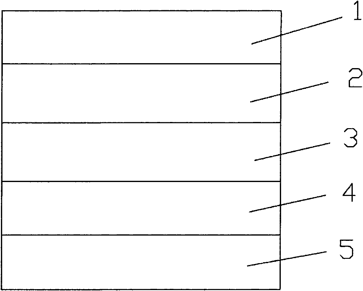
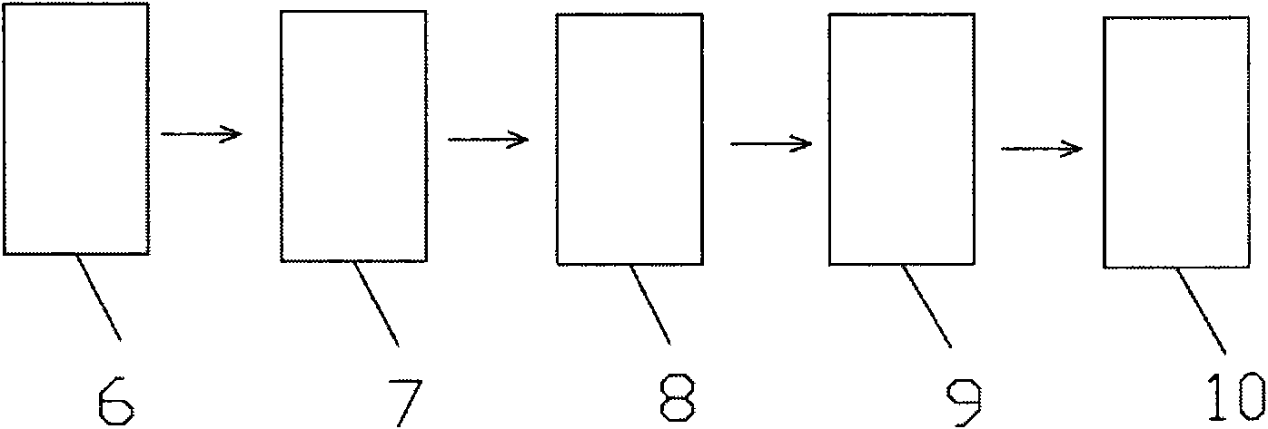
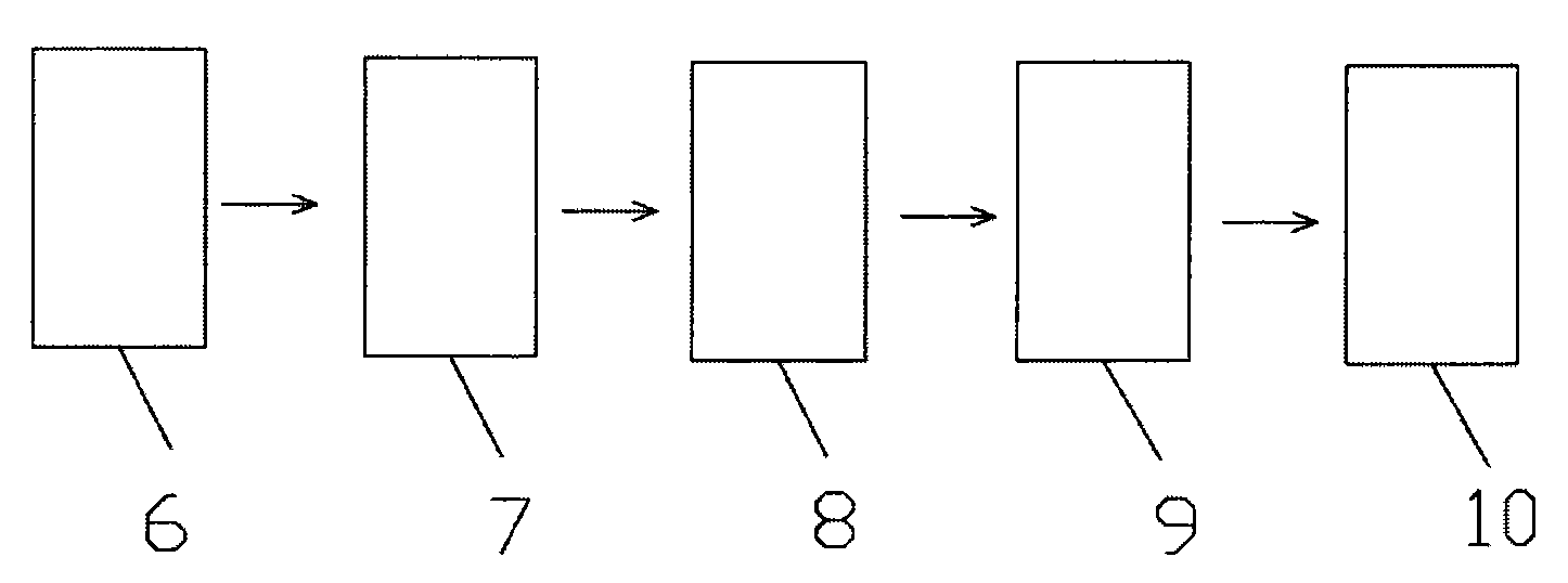
[0032] (1) Pretreatment of stainless steel substrate 5: use 0.1 cm thick stainless steel as the deposition substrate and back electrode, use acetone to ultrasonically clean for 10 minutes to remove surface grease, and then ultrasonically clean with deionized water for 10 minutes to remove impurities on the stainless steel surface , and finally put the stainless steel into the pretreatment chamber 6 after drying, and use plasma to clean the stainless steel substrate 5 .
[0033] (2) Chemical vapor growth graphite buffer layer 4: the stainless steel substrate 5 is transferred to the chemical vapor deposition furnace 7, and high-purity CH is introduced into the chemical vapor deposition chamber 4 and H 2 , the deposition temperature is 300° C., the deposition pressure is 2000 Pa, and the deposition thickness...
PUM
| Property | Measurement | Unit |
|---|---|---|
| thickness | aaaaa | aaaaa |
Abstract
Description
Claims
Application Information