Wafer-level vacuum encapsulating method for micro-electromechanical device

A technology for vacuum packaging and device wafers, which is used in microstructure devices, processing microstructure devices, metal processing mechanical parts, etc., and can solve problems such as changing the performance of anti-reflection coatings or getters, so as to reduce failure rates and avoid failures. Effect

Active Publication Date: 2010-08-11
北方广微科技有限公司
View PDF6 Cites 29 Cited by
  • Summary
  • Abstract
  • Description
  • Claims
  • Application Information

AI Technical Summary

Problems solved by technology

However, high temperature, acid, alkali, plasma, etc. may change the performance of the anti-

Method used


Image

  • Wafer-level vacuum encapsulating method for micro-electromechanical device
  • Wafer-level vacuum encapsulating method for micro-electromechanical device
  • Wafer-level vacuum encapsulating method for micro-electromechanical device

Examples


Embodiment Construction

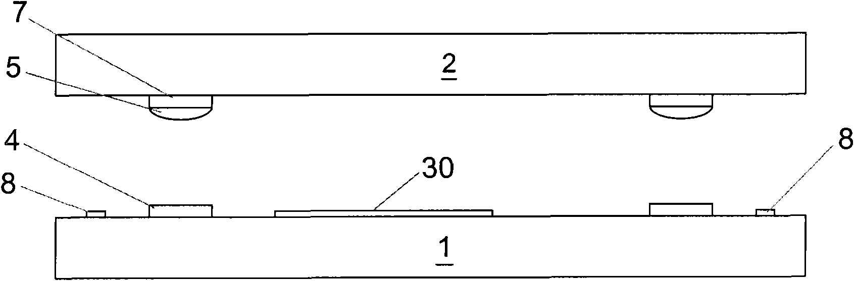
[0051] The wafer-level vacuum packaging method for micro-electromechanical devices will be described below by taking the packaging of an uncooled infrared microbolometer chip as an example.

[0052] refer to Figure 3A-Figure 3H , Figure 4 and Figure 5 . According to the method of the present invention, the wafer-level vacuum packaging method of the uncooled infrared microbolometer chip 30 includes the following steps in sequence:

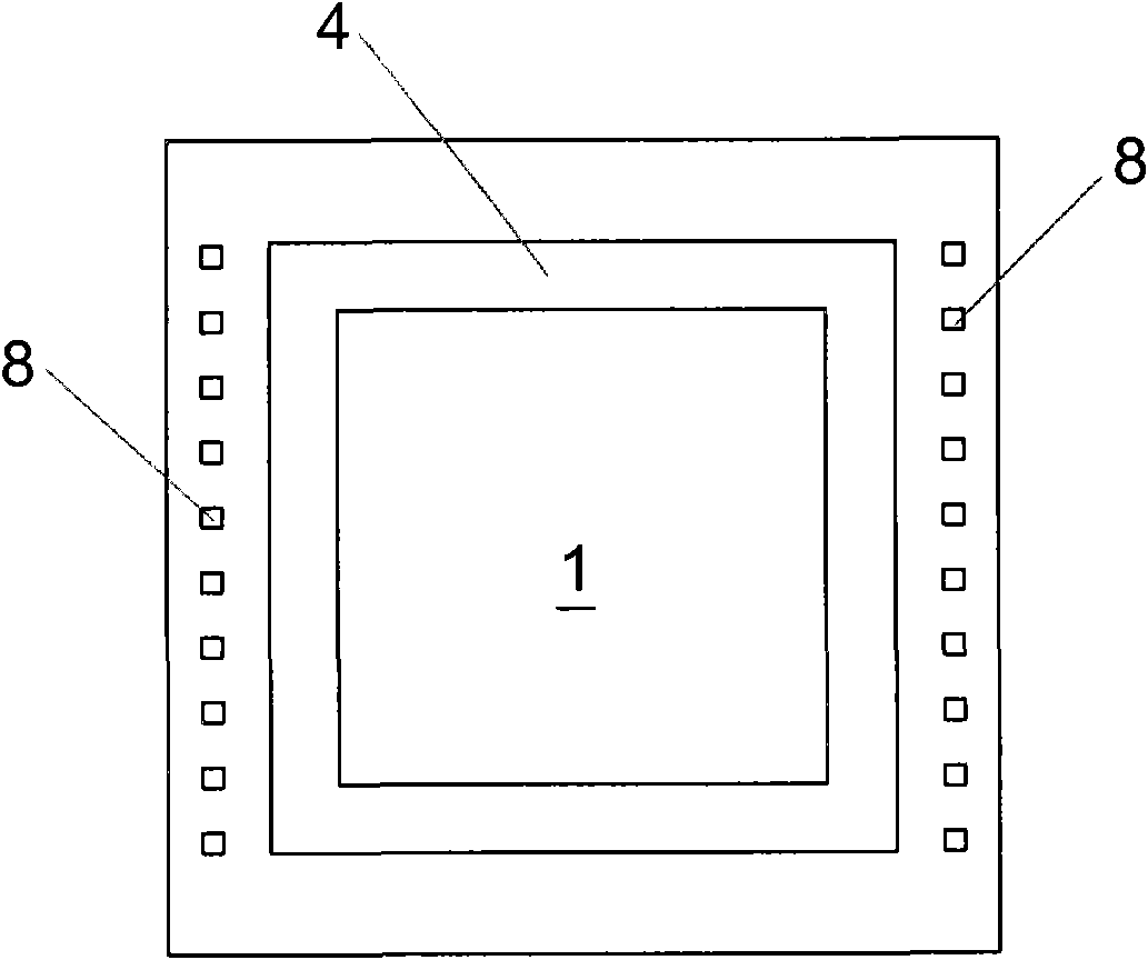
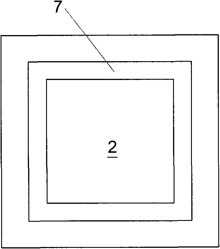
[0053] S1. Wafer preparation: Prepare capping wafer 2 and device wafer 1, wherein capping wafer 2 is silicon single crystal or germanium single crystal grown by fusion method, with crystal orientation ; device wafer 1 has been prepared There are uncooled infrared microbolometer 30 and lead plate 8.

[0054] S2. Growing sealing rings 4 and 7 on the front of the device wafer 1 and the front of the capping wafer 2 respectively, the specific steps are:

[0055] S2a. Spin-coat a photoresist (positive resist) of about 2um on the front of the devic...


PUM

PropertyMeasurementUnit
Thicknessaaaaaaaaaa
Depthaaaaaaaaaa
Depthaaaaaaaaaa

Abstract

The invention provides a wafer-level vacuum encapsulating method for a micro-electromechanical device, which comprises the following steps in turn: S1, preparing a seal cover wafer and a device wafer; S2, growing a seal ring on the fronts of the device wafer and the seal cover wafer respectively; S3, growing a solder on the seal ring on the front of the seal cover wafer; S4, performing deep silicon etching on the seal cover wafer to form a groove by using the seal ring as a mask; S5, growing a degasser film on the front of the seal cover wafer, wherein the pattern of the degasser film is directly obtained from the grown mask plate; S6, heating linkage equipment to activate the degasser film, and bonding the seal cover wafer and the device wafer together; S7, growing an anti-reflection film on the back of the seal cover wafer, wherein the pattern of the anti-reflection film is directly obtained from the grown mask plate; and S8, cutting flakes. The method avoids the influence of the post process on the previous process by adjusting the sequence of the processes, and is particularly suitable for encapsulating infrared devices.

Description

technical field [0001] The invention relates to a wafer-level vacuum packaging method for a micro-electromechanical device. Background technique [0002] For micro-electromechanical (MEMS) devices, the traditional packaging technology is mainly chip-level packaging. The process flow includes the following steps: firstly prepare the MEMS chip on the silicon wafer; then slice the wafer, release the sacrificial layer, patch, lead wire; finally seal the cap. Among these steps, the steps after releasing the sacrificial layer are all performed on a single chip. Since a wafer can be diced to produce hundreds of chips, the cost of such chip-scale packaging is high. In fact, about 90% of the cost of a finished MEMS device is spent on packaging. Therefore, reducing packaging costs is a major development trend of the MEMS industry. Integrated circuits (ICs) have achieved wafer-level packaging. On the basis of referring to the wafer-level packaging technology of integrated circuits,...

Claims


Application Information

Patent Timeline
IPC IPC(8): B81C3/00
Inventor 方辉雷述宇
Owner 北方广微科技有限公司
Why Eureka
Try Eureka