Nano electron device using nanocrystal material as Coulomb island and manufacture method thereof

A technology of nanocrystalline materials and electronic devices, which is applied in the field of microelectronics, can solve the problems of complex manufacturing process, high manufacturing cost, and low operating temperature of devices, and achieve the effects of simplifying the manufacturing process, reducing manufacturing costs, and good compatibility

Active Publication Date: 2010-08-11
合肥中科微电子创新中心有限公司
View PDF0 Cites 4 Cited by
  • Summary
  • Abstract
  • Description
  • Claims
  • Application Information

AI Technical Summary

Problems solved by technology

[0006] At present, electron beam lithography and etching are mostly used to directly process the Coulomb island structure of single-electron transistors or further use oxidation methods to obtain and reduce the size of Coulomb islands, but the operating temperature of the devices prepared by this method is not high. , and generally have the disadvantages of complex manufacturing process and high manufacturing cost

Method used


Image

  • Nano electron device using nanocrystal material as Coulomb island and manufacture method thereof
  • Nano electron device using nanocrystal material as Coulomb island and manufacture method thereof
  • Nano electron device using nanocrystal material as Coulomb island and manufacture method thereof

Examples


Embodiment Construction

[0033] In order to make the object, technical solution and advantages of the present invention clearer, the present invention will be described in further detail below in conjunction with specific embodiments and with reference to the accompanying drawings.

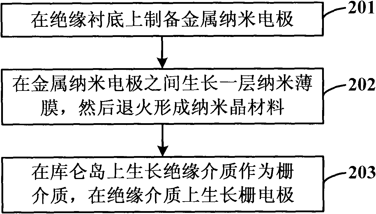
[0034] Such as figure 2 as shown, figure 2 It is a flow chart of a method for making nanoelectronic devices using nanocrystalline materials as Coulomb islands provided by the present invention, the method comprising:

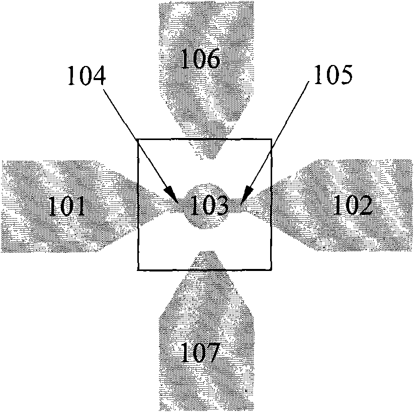
[0035] Step 201: preparing metal nano-electrodes on an insulating substrate by electron beam lithography, metal deposition and lift-off processes;

[0036] Step 202: Using one of sputtering, evaporation, and atomic layer deposition to grow a layer of Si, Ni, Cu, Al, Pt, Au, Ag, W, Ti with a thickness of 1 nm to 3 nm between the nano electrodes , Cr, WTi thin films, and then annealed in nitrogen at a temperature of 600 ° C to 1300 ° C for 10 seconds to 30 seconds to form nanocrystalline materials;

[00...


PUM

PropertyMeasurementUnit
Thicknessaaaaaaaaaa
Diameteraaaaaaaaaa
Thicknessaaaaaaaaaa

Abstract

The invention discloses a nano electron device using a nanocrystal material as a Coulomb island and a manufacture method thereof. A pair of nano electrodes is manufactured on a substrate; the nanocrystal material grows between the pair of nano electrodes; the nano electrodes are used as the source and the drain of the device; the nanocrystal is used as the Coulomb island; insulating media growingon the Coulomb island are used as grid media; and electrodes on the insulating media are used as grid electrodes. The nano electron device and the manufacture method thereof have the advantages of simplicity, stability, reliability and few processing steps and are compatible with traditional CMOS processes.

Description

technical field [0001] The invention belongs to the technical field of microelectronics, relates to a nanoelectronic device and a nanoprocessing technology, in particular to a nanoelectronic device using a nanocrystalline material as a Coulomb island and a manufacturing method thereof. Background technique [0002] Integrated circuits with complementary metal-oxide-semiconductor (CMOS) devices as the mainstream technology have been developing rapidly following Moore's Law. In 2004, integrated circuits entered the 90-nanometer technology node. As the feature size enters the nanoscale, the traditional CMOS technology is facing more and more serious challenges. Therefore, nanoelectronic devices based on new principles have become a research hotspot. [0003] Single-electron transistor is a typical nanoelectronic device, which has the advantages of small size, fast speed, low power consumption, and large-scale integration, and has very broad application prospects, such as making...

Claims


Application Information

Patent Timeline
IPC IPC(8): H01L29/772H01L21/336
Inventor 龙世兵刘明李维龙贾锐
Owner 合肥中科微电子创新中心有限公司
Why Eureka
Try Eureka