Process for texturing crystalline silicon solar cell by dry etching

A solar cell and dry etching technology, which is applied in sustainable manufacturing/processing, circuits, photovoltaic power generation, etc., can solve the problem of difficulty in controlling the size and shape of the suede on the silicon surface, large reflection loss on the surface of solar cells, and low external quantum efficiency and other issues to achieve the effect of improving external quantum efficiency, high cell photoelectric conversion efficiency, and reducing environmental pollution

Inactive Publication Date: 2010-08-11
山东力诺太阳能电力股份有限公司
View PDF0 Cites 27 Cited by
  • Summary
  • Abstract
  • Description
  • Claims
  • Application Information

AI Technical Summary

Problems solved by technology

[0003] In order to effectively reduce the reflection on the surface of crystalline silicon and improve the light trapping effect, the preparation of textured surface is a very feasible process. At present, the wet method of textured technology is generally used in the industrial production of crystalline silicon solar cells to make the textured surface structure of the battery surface, such as using alkaline solution The surface reflectance of monocrystalline silicon textured surface can be controlled at about 12%; the surface reflectance of polycrystalline textured surface can be controlled at about 21% by using acid solution system. In this case, the surface reflection loss of solar cells is very large. , the external quantum efficiency is low, the size and shape of the suede on the silicon surface are not easy to control, and the use of a large amount of corrosive and toxic chemicals has also brought damage to the environment

Method used


Image

  • Process for texturing crystalline silicon solar cell by dry etching
  • Process for texturing crystalline silicon solar cell by dry etching
  • Process for texturing crystalline silicon solar cell by dry etching

Examples


Embodiment Construction

[0022] In order to better understand the present invention, the technical solution of the present invention will be described in detail below with specific examples, but the invention is not limited thereto.

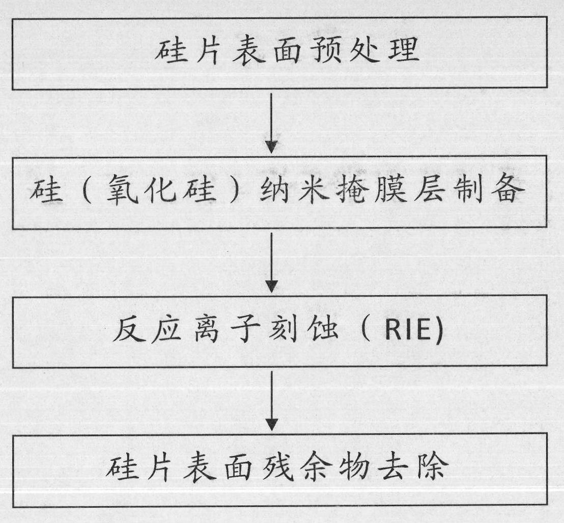
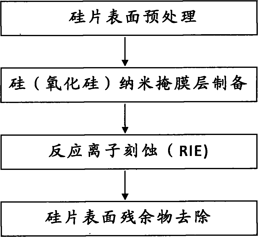
[0023] A dry etching texturing process for crystalline silicon solar cells of the present invention, the technical proposal is: a dry etching texturing process for crystalline silicon solar cells, comprising a silicon chip surface pretreatment step, reactive ion etching (RIE) Step, the silicon wafer surface residue removal step after etching, after the silicon wafer surface is pretreated, a nano-mask layer is prepared on the silicon wafer surface, and then the silicon wafer with the nano-mask layer is carried out by reactive ion etching ( RIE), after removing surface residues at last, a suede surface is formed on the surface of the silicon wafer.

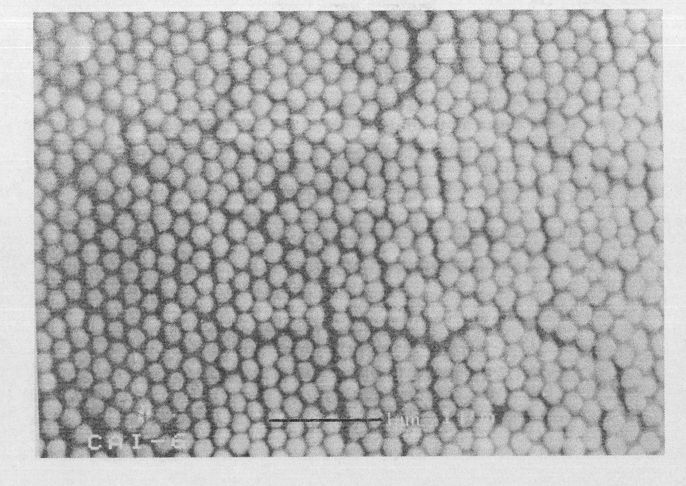
[0024] The nano-mask layer is a monodisperse layer of silicon or silicon dioxide nanospheres.

[0025] The specific steps a...


PUM

PropertyMeasurementUnit
particle diameteraaaaaaaaaa

Abstract

The invention relates to a process for texturing a crystalline silicon solar cell by dry etching, belonging to the technical filed of the solar cell texturing. The process for texturing the crystalline silicon solar cell by dry etching comprises the following steps of pre-processing the surface of a silicon wafer, preparing a layer of nano masking film on the surface of the silicon wafer, carrying out the reactive ion etching (RIE) for the silicon wafer with the nano masking film, removing the residues on the surface of the silicon wafer and texturing the surface of the silicon wafer. After the surface of the silicon wafer is textured, the reflectivity of the surface of the silicon wafer can be reduced to less than 2 percent, and the light absorption rate can be improved. Compared with the traditional technology for texturing the crystalline silicon solar cell by wet chemical etching, the process for texturing the crystalline silicon solar cell by dry etching can ensure that crystalline silicon solar cell has higher photoelectric conversion efficiency and can reduce the environmental pollution caused by texturing the crystalline silicon solar cell and is suitable for the industrial production of the crystalline silicon solar cell.

Description

technical field [0001] The invention belongs to the technical field of solar cell texturing, and in particular relates to a dry etching texturing process for crystalline silicon solar cells. Background technique [0002] With the depletion of traditional energy sources and rising oil prices, as well as the continuous improvement of people's environmental requirements, as a non-polluting clean energy, the development of solar cells is extremely rapid. As a crystalline silicon solar cell that occupies most of the solar cell market today, its preparation technology has always represented the preparation technology level of the entire solar cell industry. For example, improving the conversion efficiency is one of the key topics in solar cell research, and effectively reducing the reflection loss of sunlight on the surface of crystalline silicon wafers is an important method to improve the conversion efficiency of solar cells. [0003] In order to effectively reduce the reflecti...

Claims


Application Information

Patent Timeline
Patent Type & Authority Applications(China)
IPC IPC(8): H01L31/18H01L31/0236
CPCY02E10/50Y02P70/50
Inventor 焦云峰杨青天程谦礼
Owner 山东力诺太阳能电力股份有限公司
Why Eureka
Try Eureka