Method for preparing longitudinal high-pressure deep-slot transistor

A technology of semiconductor tubes and semiconductors, which is applied in the field of preparation of silicon-made vertical high-voltage deep-groove metal oxide semiconductor field-effect transistors, can solve the problems of high device performance, low process cost, and high process controllability, so as to improve reliability, The effect of improving performance

Inactive Publication Date: 2010-08-25
SUZHOU POWERON IC DESIGN
View PDF0 Cites 9 Cited by
  • Summary
  • Abstract
  • Description
  • Claims
  • Application Information

AI Technical Summary

Problems solved by technology

[0004] Aiming at the problems encountered in the preparation method of the structure of the vertical double-diffused metal-oxide-semiconductor field-effect transistor with the PN spacer structure in the drift region made of silicon, the present invention proposes a vertical high-voltage transistor made by groove etching and groove filling processes. A method for preparing a deep-groove semiconductor tube. This method has high process controllability, low process cost, and high performance of the manufactured device.

Method used


Image

  • Method for preparing longitudinal high-pressure deep-slot transistor
  • Method for preparing longitudinal high-pressure deep-slot transistor
  • Method for preparing longitudinal high-pressure deep-slot transistor

Examples


Embodiment 1

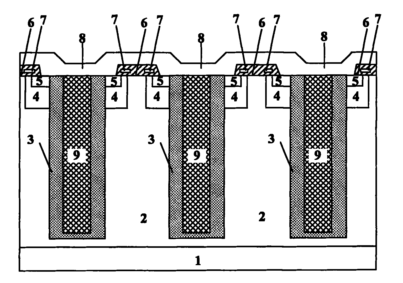
[0022] Referring to Figures 1-8, a method for manufacturing a vertical high-voltage deep-groove semiconductor tube includes the following steps:

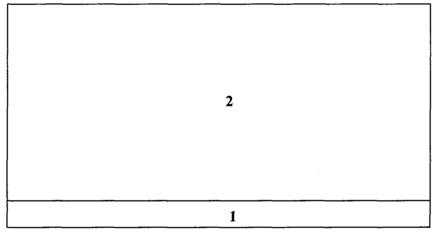
[0023] As shown in FIG. 1 : an N-type doped substrate is taken, and an N-type epitaxial layer is grown by a known epitaxial growth process.

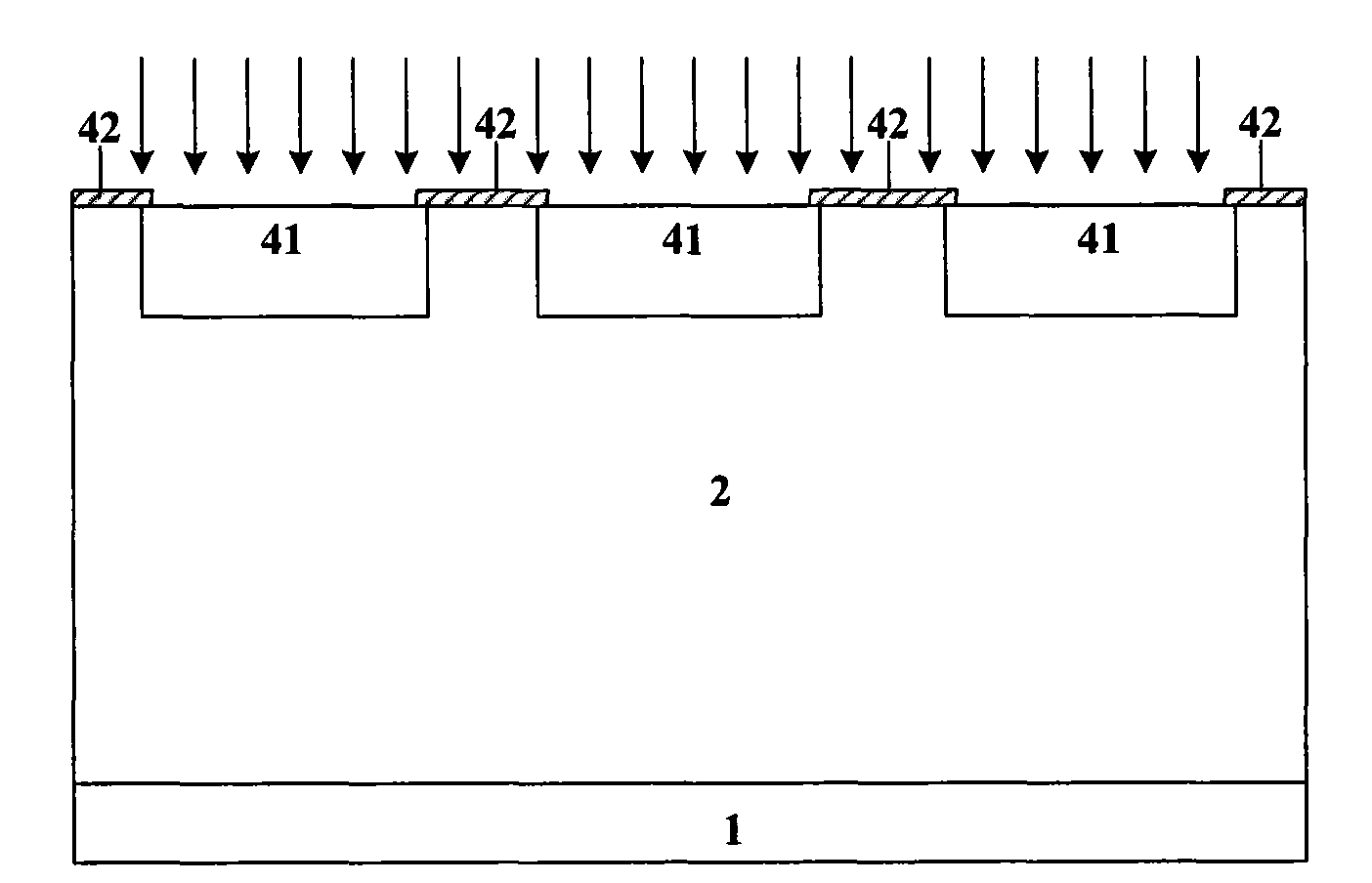
[0024] As shown in FIG. 2 , a P-type doped semiconductor region 4 is formed by using a mask plate 42 and using known ion implantation and annealing processes.

[0025] As shown in FIG. 3 , a deep groove 51 is formed in the N-type epitaxial layer 2 by a known deep groove etching process.

[0026] As shown in Fig. 4, molten borophosphosilicate glass 19 is then filled into the deep groove.

[0027] As shown in Figure 5, the borophosphosilicate glass on the surface of the device is removed by a known chemical vapor polishing process, and then the boron impurities and phosphorus impurities in the borophosphosilicate glass are diffused to the side walls of the deep groove by a known annealing push-...

Embodiment 2

[0037] An N-type doped substrate is taken, and an N-type epitaxial layer is grown by a known epitaxial growth process. The concentration of the N-type epitaxy is 1015cm-3, then use the mask 42, adopt the known ion implantation and annealing process to form the P-type doped semiconductor region 4, and then use the known deep groove etching process in the N-type epitaxial layer 2 Deep grooves 51 are formed. The molten borophosphosilicate glass 19 is then filled into the deep groove. And the content of the phosphorus source in the borophosphosilicate glass 19 is controlled within 1014, and the content of the phosphorus source is slightly higher than it can be. Then the borophosphosilicate glass on the surface of the device is removed by the known chemical vapor polishing process, and then the known The annealing push-well process makes the boron and phosphorus impurities in the borophosphosilicate glass diffuse into the silicon on the sidewall and bottom of the deep trench, maki...


PUM


Abstract

The invention discloses a method for preparing a longitudinal high-pressure deep-slot transistor. P-type semiconductor regions and N-type semiconductor regions are alternatively arrayed in a drift region of a device. The P-type semiconductors in the drift region are prepared by the steps of: firstly, forming deep slots by using a deep-slot etching process; secondly, filling boron-phosphorosilicate glass into the deep slots; thirdly, removing the boron-phosphorosilicate glass from the surface by etching; and finally, diffusing boron impurities and phosphorus impurities in the boron-phosphorosilicate glass into silicon on the side walls and at the bottoms of the deep slots by using an annealing process, wherein the boron impurity content of the boron-phosphorosilicate glass is far more than the phosphorus impurity content, so that the semiconductor regions on the side walls and at the bottoms of the deep slots are changed into the P-type doped semiconductor regions. The method has high process controllability and low process cost, and the manufactured device has high performance.

Description

Technical field: [0001] The invention relates to a method for preparing a high-voltage power metal oxide semiconductor device made of silicon, more precisely, a method for preparing a vertical high-voltage deep groove metal oxide semiconductor field effect transistor made of silicon. Background technique: [0002] At present, power devices are more and more widely used in daily life, industrial production and other fields, especially power metal oxide semiconductor field effect transistors, which have more advantages than power bipolar devices. The use of power metal oxide semiconductor tubes in power applications has the following advantages: First, the driving circuit of power metal oxide semiconductor tubes is relatively simple. Bipolar transistors may require as much as 20% of the rated collector current to ensure saturation, while MOS transistors require much less drive current and can often be driven directly by CMOS transistors or collectors. Open-circuit transistor-...

Claims


Application Information

Patent Timeline
Patent Type & Authority Applications(China)
IPC IPC(8): H01L21/336H01L21/20H01L21/8234
Inventor 易扬波李海松王钦刘侠陶平
Owner SUZHOU POWERON IC DESIGN
Why Eureka
Try Eureka