Method for preparing top gate top contact self-alignment Organic Thin Film Transistor (OTFT)
An organic thin film, top-contact technology, applied in the field of microelectronics, can solve the problems of high cost, unsuitable for making integrated circuits, expensive silicon substrates and Au electrodes, etc.
- Summary
- Abstract
- Description
- Claims
- Application Information
AI Technical Summary
Problems solved by technology
Method used
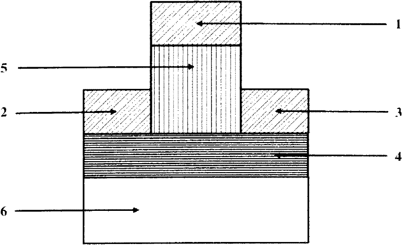
Image

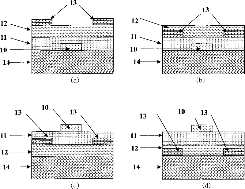
Examples
Embodiment 1
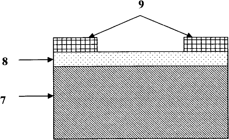
[0040] 1. Firstly, Corning 1737 glass substrate 6 with a thickness of 1mm is ultrasonicated with ethanol / acetone mixed solvent for 10 minutes to remove grease and other organic matter on the surface of the substrate. Then put the glass substrate into pure deionized water, boil it until there are no remaining bubbles on the surface of the substrate, and then ultrasonically clean it again for 10 minutes to wash away the detergent and some inorganic contaminants. Finally, rinse with deionized water ultrasonic for 10 minutes. After rinsing, place the glass substrate in a clean bench in a clean room and dry it with an infrared lamp for 2 hours to completely remove the surface moisture.
[0041] 2. Use vacuum evaporation method to grow CuPc active layer, (equipment adopts ZK-3 multi-source vacuum coating machine) The vacuum degree is 5×10 -4 Pa, the growth rate monitored by the film thickness meter is 0.4nm / s, the growth time is 150s, the active layer thickness is about 60nm, and the ev...
PUM
 Abstract
Description
Claims
Application Information
 - R&D
- Intellectual Property
- Life Sciences
- Materials
- Tech Scout
- Unparalleled Data Quality
- Higher Quality Content
- 60% Fewer Hallucinations
Browse by: Latest US Patents, China's latest patents, Technical Efficacy Thesaurus, Application Domain, Technology Topic, Popular Technical Reports.
© 2025 PatSnap. All rights reserved.Legal|Privacy policy|Modern Slavery Act Transparency Statement|Sitemap|About US| Contact US: help@patsnap.com