
Semiconductor laser

A technology of semiconductors and optical components, which is applied in the direction of semiconductor lasers, electrical components, laser components, etc., can solve problems such as single-mode degradation, and achieve high-speed response and single-mode performance, good initial characteristics and long-term reliability. Effect

Inactive Publication Date: 2010-08-25
MITSUBISHI ELECTRIC CORP
View PDF1 Cites 5 Cited by
  • Summary
  • Abstract
  • Description
  • Claims
  • Application Information

AI Technical Summary

Problems solved by technology

Therefore, in an AR / HR type semiconductor laser whose light reflectance is asymmetrical at the two facing laser end faces, there is a problem that the single-mode characteristic is degraded due to an excessively large κ L.

Method used


Image

  • Semiconductor laser
  • Semiconductor laser
  • Semiconductor laser

Examples


Embodiment approach 1

[0039] [structure]

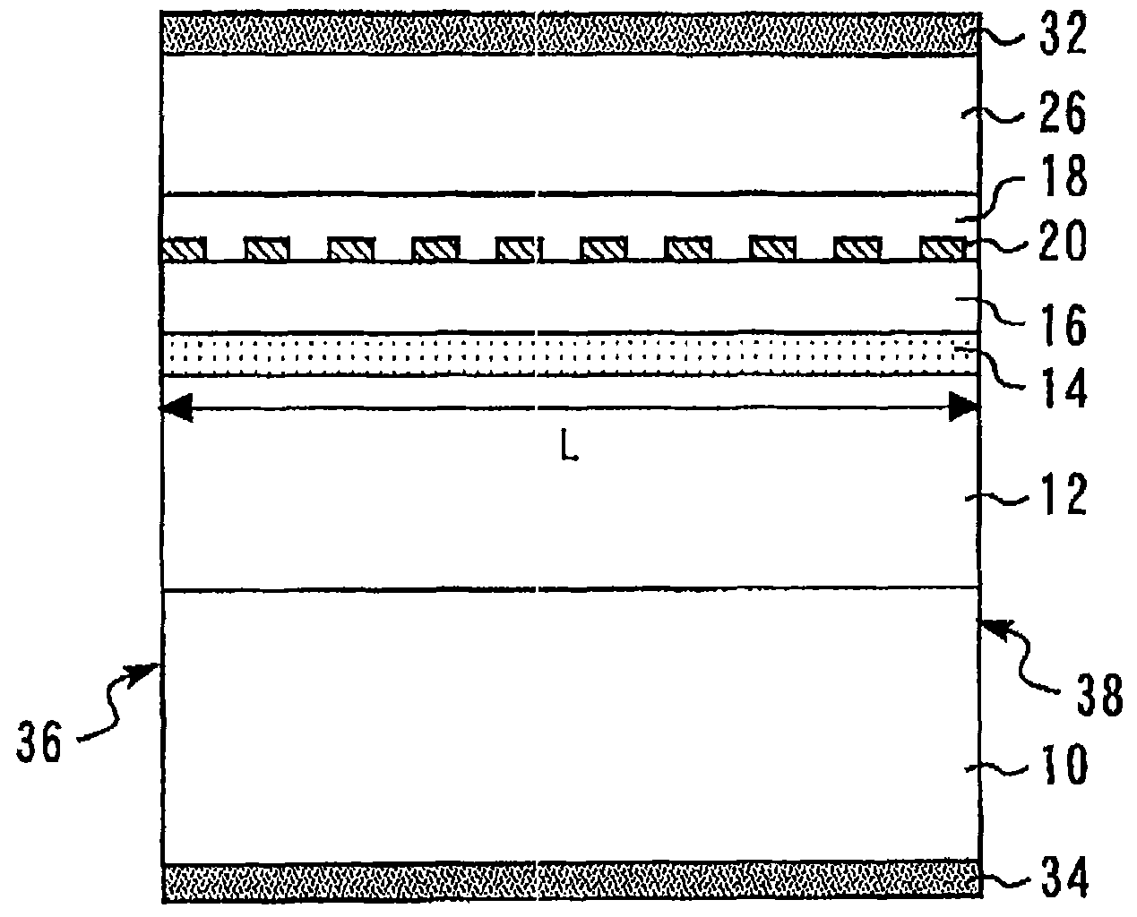
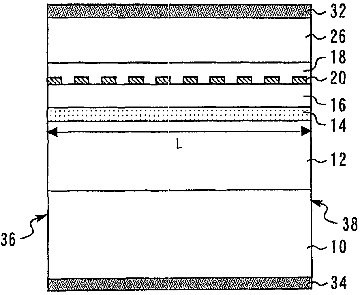
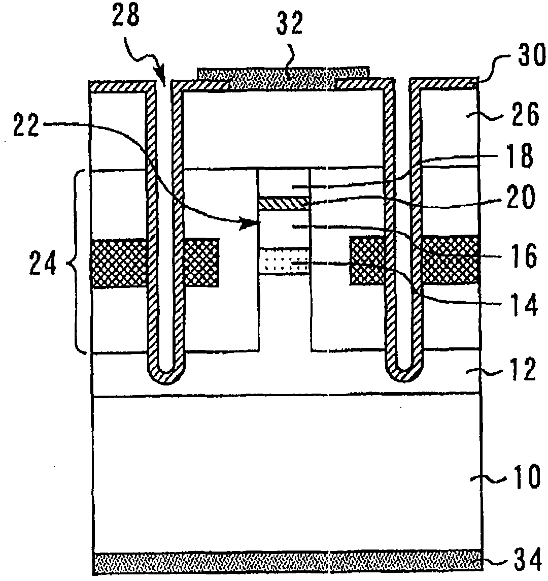
[0040] 1 and 2 are cross-sectional views showing a semiconductor optical element according to Embodiment 1. As shown in FIG. Fig. 1 is a sectional view in the direction of the optical waveguide, and Fig. 2 is a sectional view parallel to the end face of the laser. This semiconductor optical element is a distributed feedback type semiconductor laser.

[0041] On a p-type InP substrate 10, a p-type InP cladding layer 12, an active layer 14 made of InGaAsP, an n-type InP cladding layer 16, and an n-type InP layer 18 are laminated in this order. A diffraction grating 20 is formed in the n-type InP cladding layer 16 and the n-type InP layer 18 along the optical waveguide direction. The diffraction grating 20 is formed by removing an InGaAsP layer having a PL wavelength of 1200 nm or more at predetermined intervals determined by the oscillation wavelength.

[0042] Mesa 22 which is a current narrowing structure is formed in p-type InP cladding layer 12 , acti...

Embodiment approach 2

[0060] FIG. 14 is a cross-sectional view showing a semiconductor optical element according to Embodiment 2. FIG. A waveguide 48 for extracting light emitted from the semiconductor laser 46 is integrated with the semiconductor laser 46 of the first embodiment.

Embodiment approach 3

[0062] FIG. 15 is a cross-sectional view showing a semiconductor optical element according to Embodiment 3. FIG. A semiconductor optical element 50 such as a semiconductor modulator or a semiconductor optical amplifier is integrated with the semiconductor laser 46 of the first embodiment.


PUM


Abstract

The invention provides a semiconductor laser including a p-type semiconductor layer, an active layer, and an n-type semiconductor layer sequentially laminated on a p-type semiconductor substrate; and a diffraction grating in the n-type semiconductor layer along the direction of an optical waveguide. The reflectance of light on two facing laser end surfaces is asymmetric; the length L of the active layer in the optical waveguide direction is 130 mum or shorter; the diffraction grating material has a photoluminescence wavelength of 1,200 nm or longer; and kappa L, which is the product of the length L and the coupling coefficient kappa of the diffraction grating, is at least 1.5 and smaller than 3.0.

Description

technical field [0001] The present invention relates to a semiconductor optical element capable of ensuring good initial characteristics and long-term reliability and improving high-speed response and single mode performance. Background technique [0002] Semiconductor lasers used for optical communications that perform direct modulation must achieve high-speed response of about 10 Gbps even at high temperatures. Therefore, the optimization of the quantum well structure of the active layer, the high reflection achieved by coating the light exit end surface, the reduction of parasitic capacitance, the shortening of the length L of the optical waveguide direction of the active layer, and the increase of distributed feedback type or distribution A material having an Al element such as AlGaInAs is used for the coupling constant κ of the diffraction grating and the active layer in the reflective semiconductor laser. [0003] Patent Document 1: Japanese Patent Laid-Open No. 2003-...

Claims


Application Information

Patent Timeline
Patent Type & Authority Applications(China)
IPC IPC(8): H01S5/00H01S5/12
CPCH01S5/1039H01S5/3434H01S5/227H01S5/0265H01S5/026H01S5/12B82Y20/00
Inventor 境野刚
Owner MITSUBISHI ELECTRIC CORP
Learn More