

Integrated anemograph based on ceramics wafer level package and preparation method thereof
A technology of wafer-level packaging and wind speed and wind direction, which is applied to the process of producing decorative surface effects, the photolithography process of patterned surfaces, and instruments, can solve the problems of silicon wafer pollution, damage, dissipation, etc., and achieve reduction Package cost, ensure consistency, and reduce cost
Active Publication Date: 2010-09-01
SOUTHEAST UNIV
View PDF0 Cites 28 Cited by
- Summary
- Abstract
- Description
- Claims
- Application Information
AI Technical Summary
Problems solved by technology
As a result, silicon wafers are easily subject to various contaminations, resulting in unstable performance and even damage.
If a ceramic substrate with high thermal conductivity is used, and the silicon chip of the sensor is packaged by flip-chip packaging or thermally conductive adhesive, the above contradictions can be better avoided, but the heat generated by the sensor after packaging is extremely large. Part of it is dissipated from the silicon-based substrate in the form of heat conduction, and only a small part is heat-exchanged with the outside air through the ceramic, which greatly reduces the amplitude of the output sensitive signal, and the sensitive signal can be improved by increasing the power consumption of the sensor. amplitude, but it causes a large power consumption of the entire sensor system
Method used
View moreImage
Smart ImageViewing Examples

Examples
Embodiment 1
Login to View More PUM
 Abstract
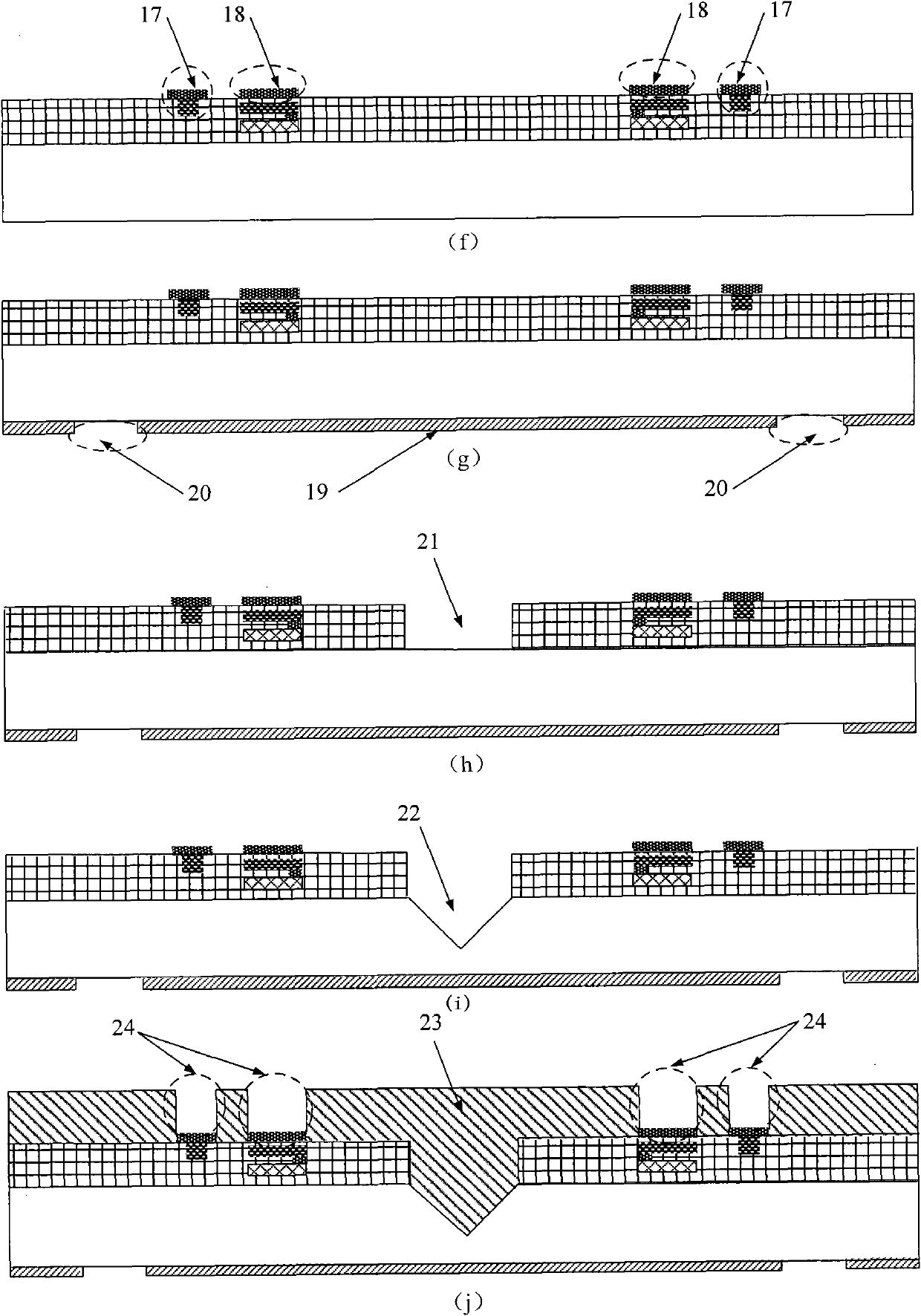
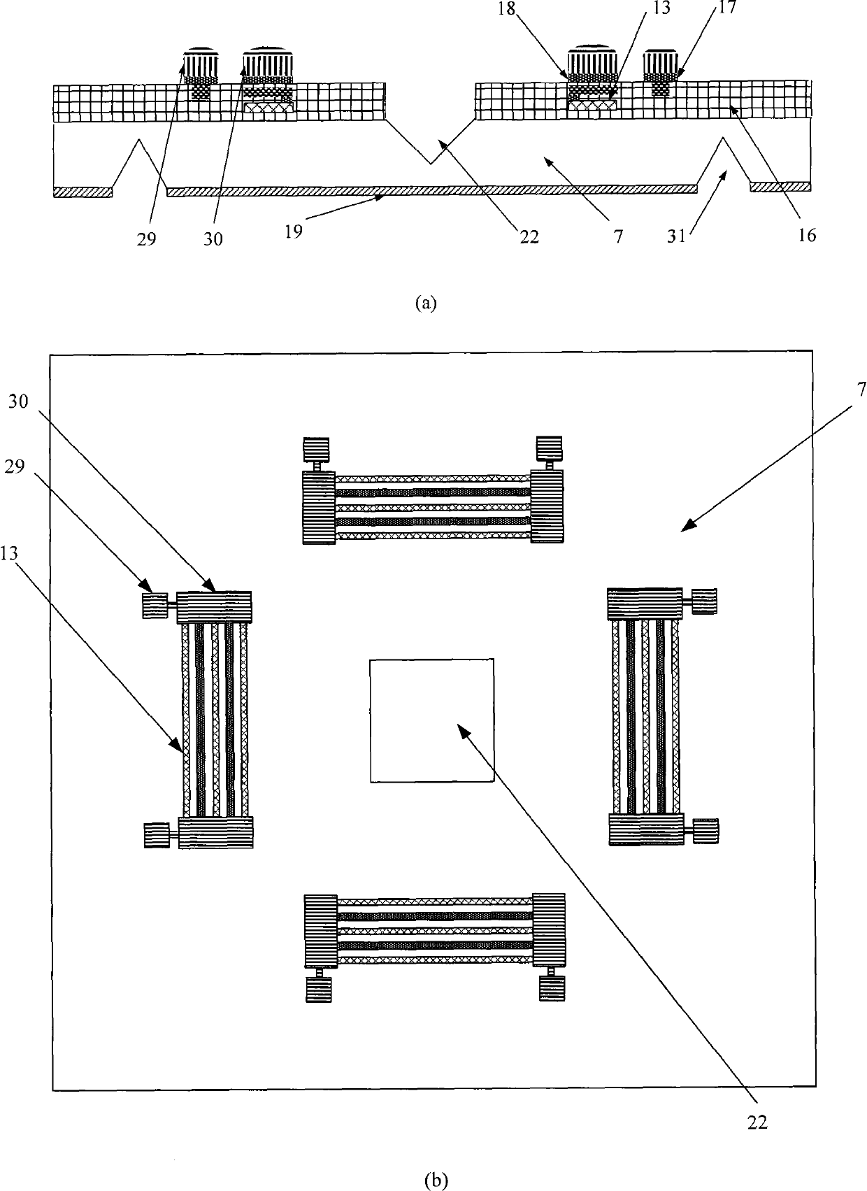
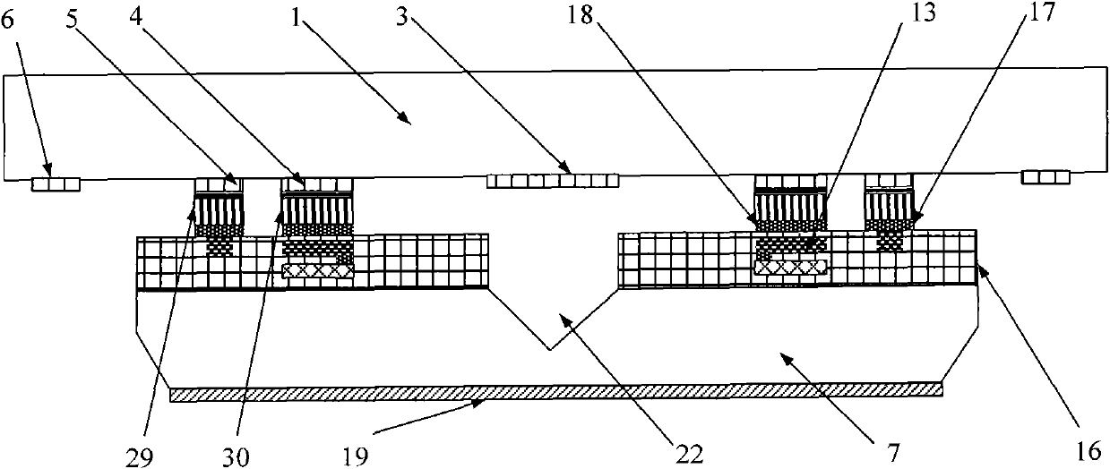
The invention discloses a preparation method of CMOS (Complementary Metal-Oxide-Semiconductor) anemograph based on ceramics wafer level package, which comprises following steps: 1, preparing a ceramics chip comprising the step of manufacturing a heating element and a pad used for electric connection, hot link and electric induction on the lower surface of the ceramics chip by a sputtering and etching technology; 2, preparing a silicon chip comprising the steps of preparing a heat sense thermometric element by a standard CMOS technology, preparing an insulation cavity and a shredding slot which is arranged at the back of the silicon chip by an MEMS (Micro-Electromechanical System) anisotropy wet etching technology and then preparing copper salient points and solder on the surface of the silicon chip; 3, realizing the mutually-connected package, electric connection and hot link between the silicon chip and the ceramics chip; 4, scribing; and 5, shredding. The invention has the advantages that the preparation method is compatible with the standard CMOS technology in the whole prepare process of the anemograph, the aftertreatment technology is simple and the wafer level package of the anemograph is realized by adopting a flip-chip bonding packaging technology, thereby having the advantages of high process consistency, good compatibility, simple aftertreatment technology and low cost.
Description
technical field The invention relates to a wind speed and direction sensor which adopts flip-chip packaging (Flip-chip) technology to realize the ceramic wafer level packaging and is compatible with the standard CMOS process, especially relates to a low power consumption ceramic wafer level packaging sensor. An integrated wind speed and direction sensor and a preparation method thereof. technical background In the design of CMOS integrated wind speed and direction sensors, packaging has always been a technical bottleneck hindering its development. On the one hand, the encapsulation material is required to have good thermal conductivity and to protect the sensor, and the impact of the encapsulation material on the sensitivity, reliability and price of the sensor needs to be considered in the design, which limits the sensor’s own encapsulation. Design freedom. On the other hand, the thermal flow sensor requires the sensitive part of the sensor to be exposed to the measuremen...
Claims
Login to View More Application Information
Patent Timeline
 IPC IPC(8): G01P5/10G01P13/00B81B7/02B81C1/00B81C3/00
Inventor董自强黄庆安秦明
OwnerSOUTHEAST UNIV