Asymmetrical 980nm semiconductor laser structure with high power and wide waveguide

An asymmetric laser technology, applied in the structure of optical waveguide semiconductors, semiconductor lasers, lasers, etc., can solve the problems of increasing device threshold current and series resistance, leaking high-order transverse modes, and limiting high-power output of lasers

Inactive Publication Date: 2010-09-01
INST OF SEMICONDUCTORS - CHINESE ACAD OF SCI
View PDF4 Cites 14 Cited by
  • Summary
  • Abstract
  • Description
  • Claims
  • Application Information

AI Technical Summary

Problems solved by technology

[0003] However, in a symmetrical waveguide structure, in order to further increase the output power of the device, it is necessary to continue to increase the thickness of the waveguide layer, which will not only lead to strong carrier leakage and the generation of high-order transverse modes, but also increase the threshold of the device Current and series resistance reduce the electro-optical conversion efficiency of the device, resulting in thermal saturation of the device, which limits the high power output of the laser

Method used


Image

  • Asymmetrical 980nm semiconductor laser structure with high power and wide waveguide
  • Asymmetrical 980nm semiconductor laser structure with high power and wide waveguide

Examples


Embodiment Construction

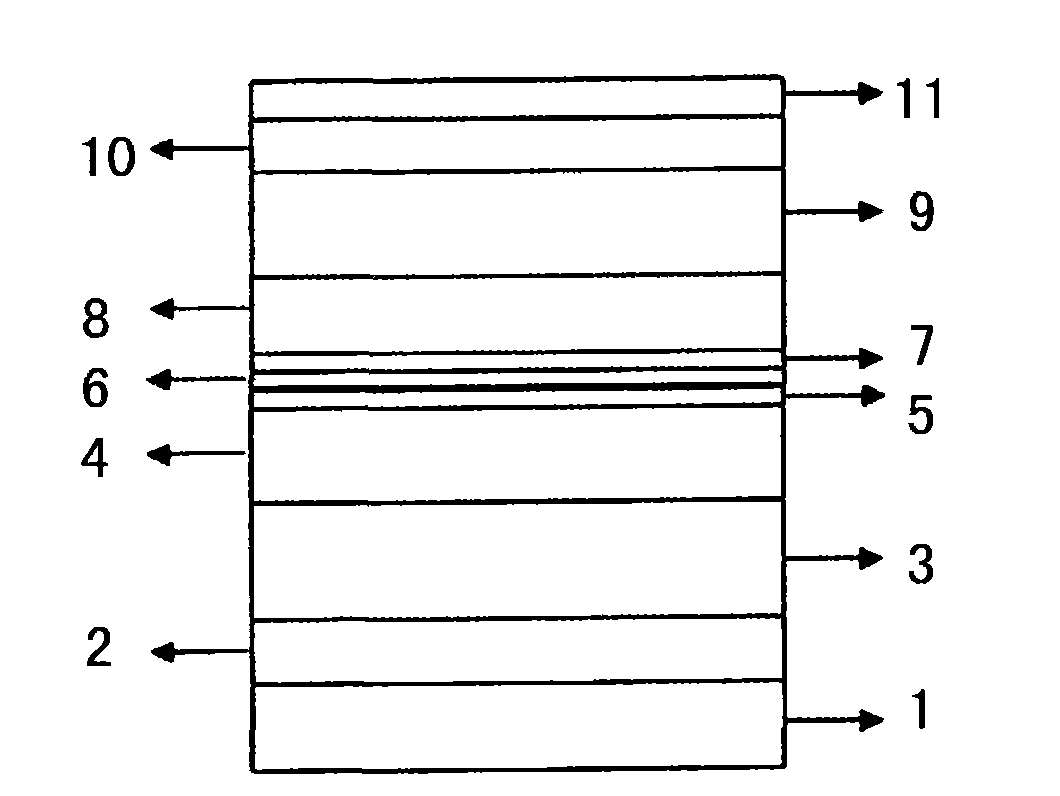
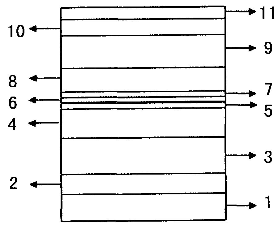
[0024] Combine below figure 1 Describe in detail the structural details of a high-power asymmetric wide-waveguide 980nm semiconductor laser according to a specific embodiment of the present invention.

[0025] refer to figure 1 , a high-power asymmetric wide waveguide 980nm semiconductor laser structure of the present invention, comprising:

[0026] A substrate 1, which is an N-type gallium arsenide material on the (100) plane, and the substrate 1 is used to epitaxially grow various layers of materials of the laser thereon;

[0027] A buffer layer 2, the buffer layer 2 is made of N-gallium arsenic material, the buffer layer 2 is fabricated on the substrate 1, and is mainly used to adjust the lattice fit;

[0028] An N-type lower confinement layer 3 is made of N-AlGaAs material, and the N-type lower confinement layer 3 is fabricated on the buffer layer 2;

[0029] The lower waveguide layer 4 is made of N-AlGaAs material, and the lower waveguide layer 4 is made on the lower c...


PUM


Abstract

The invention relates to an asymmetrical 980nm semiconductor laser structure with high power and wide waveguide, comprising a substrate, a buffer layer, an N-type lower limiting layer, a lower upper waveguide layer, a lower barrier layer, a quantum well layer, an upper barrier layer, an upper waveguide layer, a P-type upper limiting layer, a transitional layer and an electrode contact layer. The substrate is an N-type gallium arsenide material of a surface (100) and is used for the epitaxial growth of each layer material of a laser thereon; the buffer layer is made of an N-type gallium arsenide material and manufactured on the substrate; the N-type lower limiting layer is made of an N-type gallium aluminum arsenide material and manufactured on the buffer layer; the lower waveguide layer is made of an N-type gallium aluminum arsenide material and manufactured on the lower limiting layer; the lower barrier layer is made of gallium phosphorus arsenide material and manufactured on the lower waveguide layer; the quantum well layer is manufactured on the lower barrier layer; the upper barrier layer is manufactured on the quantum well layer; the upper waveguide layer is manufactured on the upper barrier layer; the P-type upper limiting layer is made of a P-type gallium aluminum arsenide material and manufactured on the upper waveguide layer; the transitional layer is made of a gallium arsenide material and manufactured on the P-type upper limiting layer; and the electrode contact layer is made of a gallium arsenide material and manufactured on the transitional layer.

Description

technical field [0001] The invention relates to the technical field of semiconductor lasers, in particular to a high-power asymmetric wide waveguide 980nm semiconductor laser structure. Background technique [0002] 980nm semiconductor lasers have very wide and important applications in the fields of material processing, laser medical treatment, and pumping solid-state lasers. In these applications, lasers are often required to have high output power. In order to obtain stable high power output, large optical cavity or even ultra-large optical cavity structures are commonly used at present. This structure has a large equivalent lateral spot size, so it can obtain high output optical power before optical catastrophe damage occurs on the cavity surface. [0003] However, in a symmetrical waveguide structure, in order to further increase the output power of the device, it is necessary to continue to increase the thickness of the waveguide layer, which will not only lead to st...

Claims


Application Information

Patent Timeline
Patent Type & Authority Applications(China)
IPC IPC(8): H01S5/343H01S5/20H01S5/06
Inventor 王冠王俊崇锋马骁宇
Owner INST OF SEMICONDUCTORS - CHINESE ACAD OF SCI
Why Eureka
Try Eureka