Method for forming dual-depth trench

A double-depth, groove technology, applied in the direction of electrical components, semiconductor/solid-state device manufacturing, circuits, etc., can solve problems such as gaps, device manufacturing yield reduction, device failure, etc., to improve fill factor, improve device yield, The effect of increasing the area of ​​the active region

Inactive Publication Date: 2010-09-08
SEMICON MFG INT (SHANGHAI) CORP +1
View PDF1 Cites 13 Cited by
  • Summary
  • Abstract
  • Description
  • Claims
  • Application Information

AI Technical Summary

Problems solved by technology

Under the existing process basis, reducing the interval of the isolation region will lead to an increase in the aspect ratio of the trench (Aspect ratio, A/R) or a reduction in the depth of the trench, and increasing the aspect ratio of the trench will make the subseq

Method used


Image

  • Method for forming dual-depth trench
  • Method for forming dual-depth trench
  • Method for forming dual-depth trench

Examples


Embodiment Construction

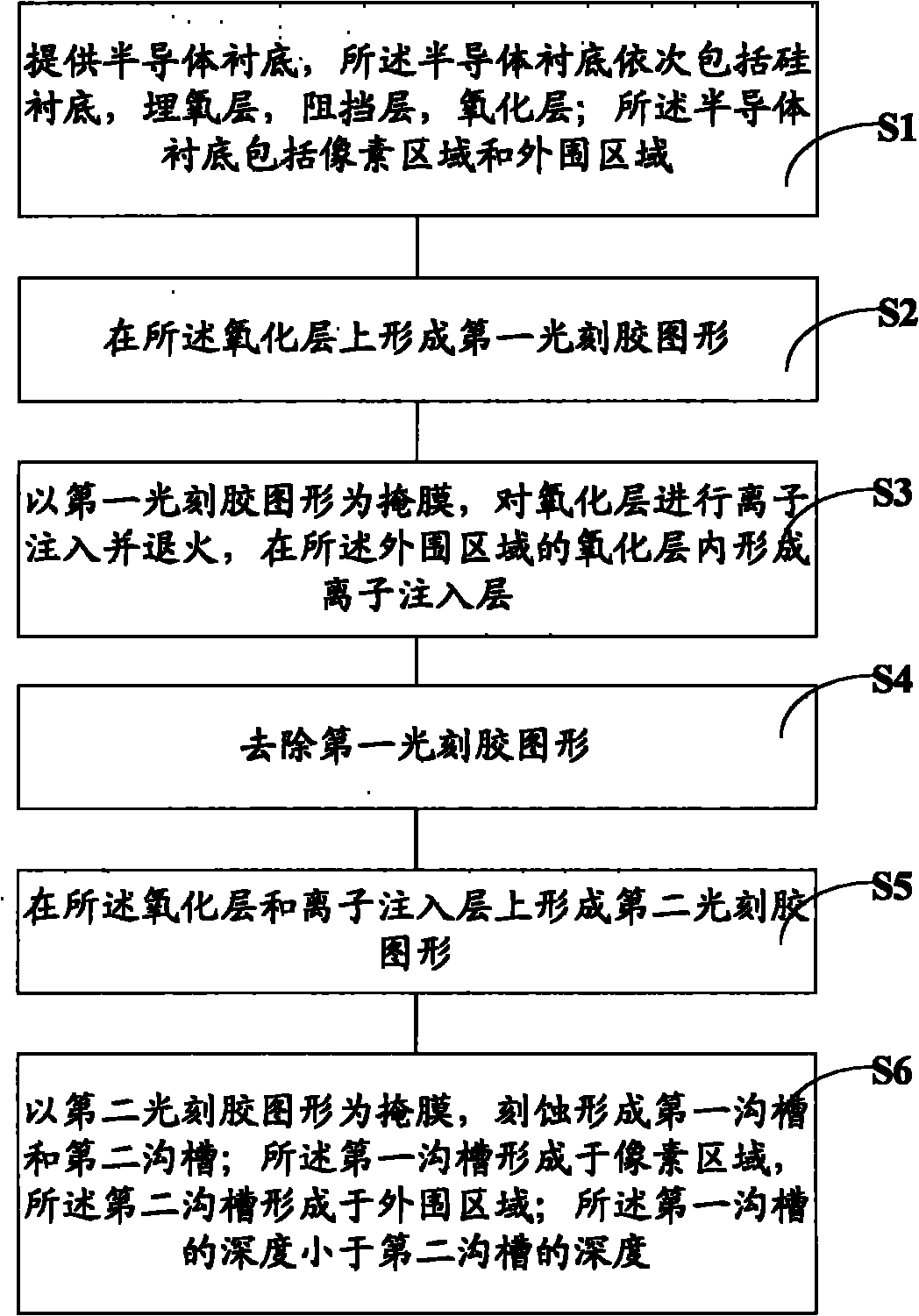
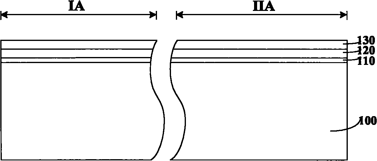
[0011] The invention provides a method for forming a double-depth trench, comprising: providing a semiconductor substrate, the semiconductor substrate sequentially includes a silicon substrate, a buried oxide layer, a barrier layer, and an oxide layer; the semiconductor substrate includes a pixel region and a peripheral region; forming a photoresist pattern on the oxide layer; using the photoresist pattern as a mask, performing ion implantation and annealing on the oxide layer, forming an ion implantation layer in the oxide layer in the peripheral region; etching the oxide layer , barrier layer, buried oxide layer and silicon substrate form a first trench and a second trench; the depth of the first trench is smaller than the depth of the second trench.

[0012] The specific embodiment of the present invention for forming double-depth grooves will be described in detail below with reference to the accompanying drawings.

[0013] refer to figure 2 , an embodiment of the presen...


PUM


Abstract

The utility model relates to a method for forming a dual-depth trench, which includes the steps that: a semiconductor substrate, which sequentially consists of a silicon substrate, a buried oxide layer, a barrier layer and an oxide layer, is provided; the semiconductor substrate comprises a pixel area and a peripheral area; a photoresist pattern is formed on the oxide layer; with the photoresist pattern as a mask, the oxide layer is implanted with ions and annealed, so that an ion-implanted layer is formed in the oxide layer of the peripheral area; the oxide layer, the barrier layer, the buried oxide layer and the silicon substrate are etched, so that a first trench and a second trench are formed; and the depth of the first trench is smaller than the depth of the second trench. The invention can effectively increase the image quality of a CMOS image sensor.

Description

technical field [0001] The invention relates to the field of semiconductor manufacturing, in particular to a method for forming double-depth trenches. Background technique [0002] At present, the charge coupled device (CCD) is the main practical solid-state image sensing device, which has the advantages of low read noise, large dynamic range, and high response sensitivity. The disadvantage of Complementary-Metal-Oxide-Semiconductor (CMOS) technology compatibility is that it is difficult to achieve single-chip integration for image sensors based on charge-coupled devices. The CMOS image sensor (CMOS Imagesensor, CIS) can integrate the pixel array and peripheral circuits on the same chip because of the same CMOS technology. Compared with the charge-coupled device, the CMOS image sensor has small size, light weight, low power consumption Low cost, convenient programming, easy control and low average cost. [0003] In general, existing image sensor technology can be found in ...

Claims


Application Information

Patent Timeline
IPC IPC(8): H01L21/762H01L21/265H01L21/311H01L27/146
Inventor 罗飞邹立
Owner SEMICON MFG INT (SHANGHAI) CORP
Why Eureka
Try Eureka