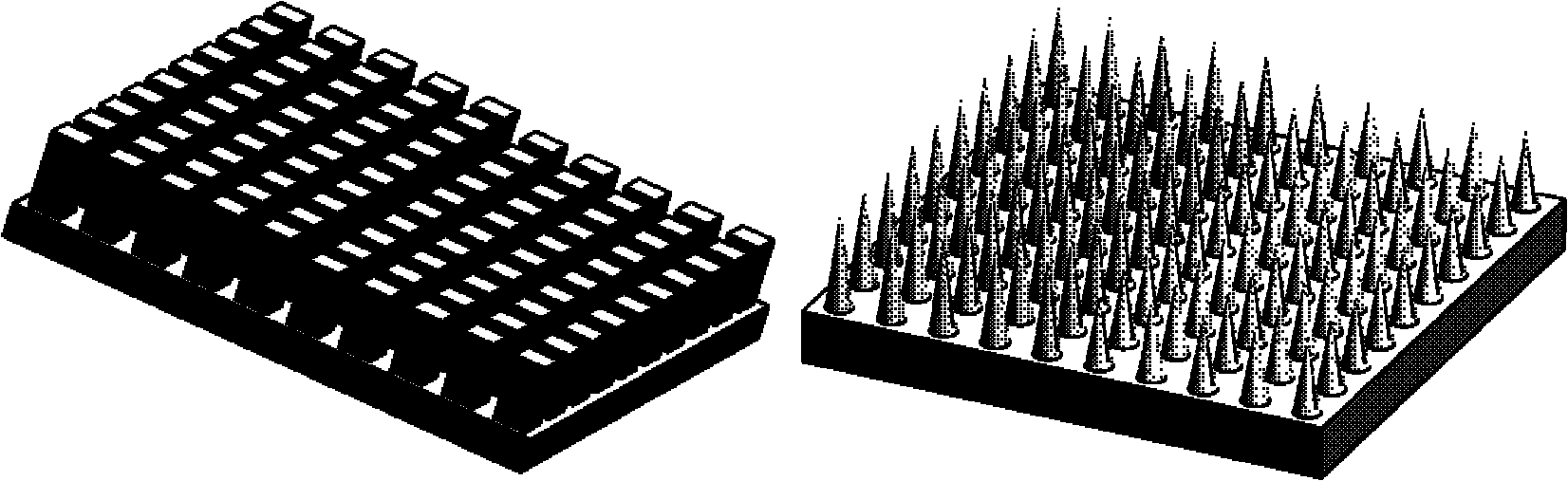
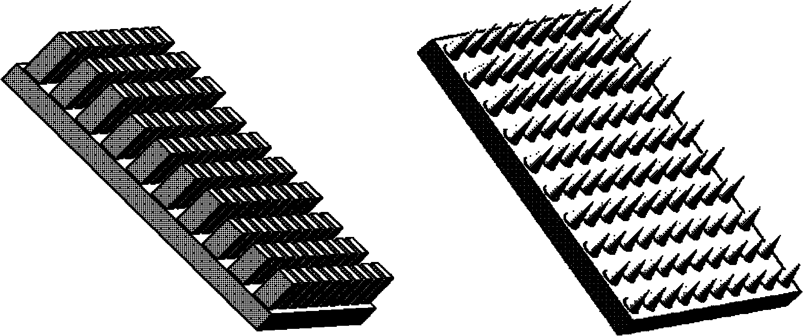
Method for preparing step micro-needle array
A technology of microneedle array and step, applied in microneedle, pattern surface photoengraving process, needle head, etc., can solve the problems of high cost and large skin resistance, and achieve the effect of reducing penetration resistance and cost.
- Summary
- Abstract
- Description
- Claims
- Application Information
AI Technical Summary
Problems solved by technology
Method used
Image

Examples
Embodiment 1
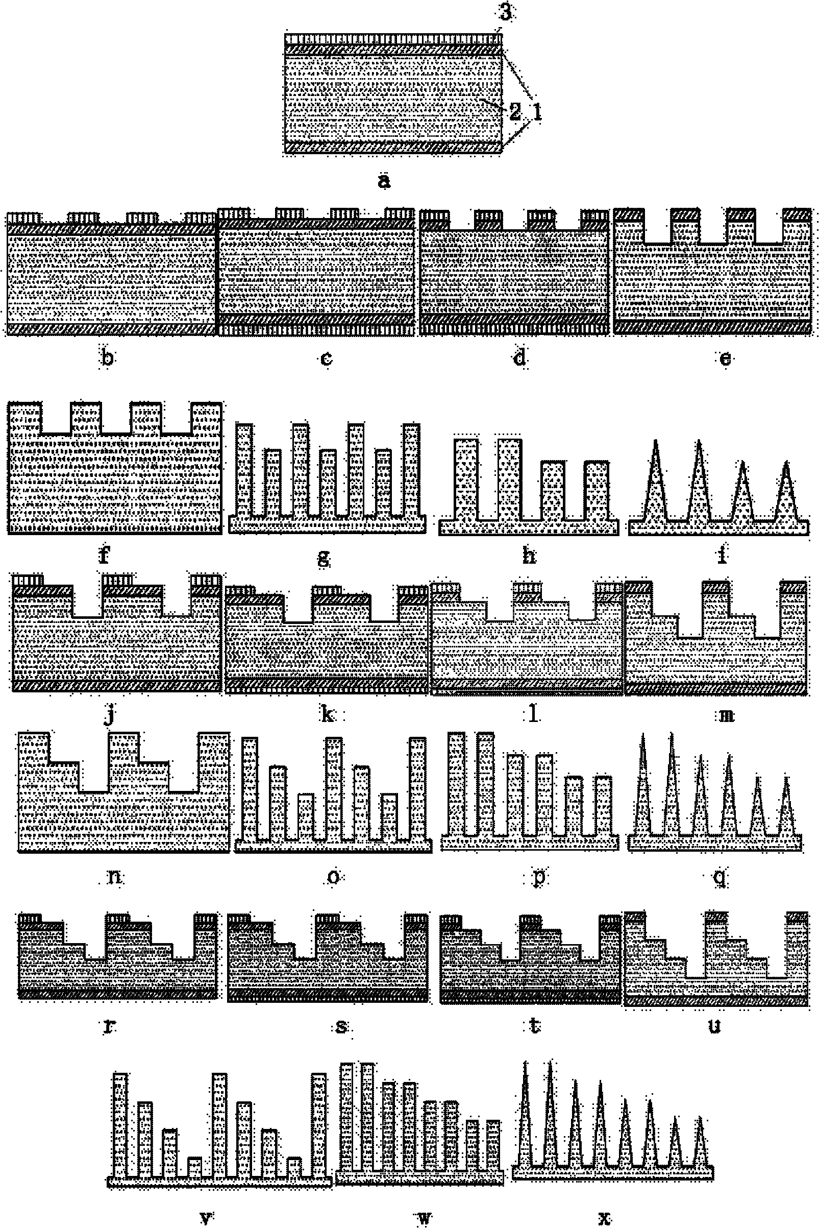
[0025] like figure 1 As shown, this embodiment includes the following steps:
[0026] A double-polished silicon oxide wafer with a thickness of 1.1mm and a diameter of 75mm was baked in an oven at 180°C for 3 hours, and then coated with a photoresist positive resist of 5 μm on the front of the double-polished silicon oxide wafer, and then baked at 95°C for 30 minutes. figure 1 As shown in a, wherein: silicon dioxide 1 is located on both sides of silicon 2, its thickness is 2-3 μm, and 3 is photoresist positive resist;
[0027] 2. Use the mask plate of the target pattern to expose, and open the photoresist positive window after development, such as figure 1 As shown in b,
[0028] 3. Bake the double-polished silicon oxide wafer again at 90°C for 30 minutes, and then cast a layer of photolithographic positive resist on the back of the double-polished silicon oxide wafer with a thickness of 5 μm, and then bake at 95°C for 30 minutes. figure 1 as shown in c;
[0029] 4. Bake t...
Embodiment 2
[0042] A double-polished silicon oxide wafer with a thickness of 1.1mm and a diameter of 75mm was baked in an oven at 180°C for 3 hours, and then coated with a photoresist positive resist of 5 μm on the front of the double-polished silicon oxide wafer, and then baked at 95°C for 30 minutes. figure 1 As shown in a, wherein: the silicon dioxide layer 1 is located on both sides of the silicon 2, and its thickness is 2-3 μm, and 3 is a positive photoresist;
[0043] 2. Use the mask plate with the target pattern to expose, and open the photoresist positive window after development, such as figure 1 as shown in b;
[0044] 3. Bake the double-polished silicon oxide wafer again at 90°C for 30 minutes, and then cast a layer of photolithographic positive resist on the back of the double-polished silicon oxide wafer with a thickness of 5 μm, and then bake at 95°C for 30 minutes. figure 1 as shown in c;
[0045] 4. Bake the double-polished silicon oxide wafer coated with photoresist on ...
Embodiment 3
[0063] A double-polished silicon oxide wafer with a thickness of 1.1mm and a diameter of 75mm was baked in an oven at 180°C for 3 hours, and then coated with a photoresist positive resist of 5 μm on the front of the double-polished silicon oxide wafer, and then baked at 95°C for 30 minutes. figure 1 As shown in a, wherein: the silicon dioxide layer 1 is located on both sides of the silicon 2, and its thickness is 2-3 μm, and 3 is a positive photoresist;
[0064] 2. Use the mask plate of the target pattern to expose, and open the photoresist positive window after development, such as figure 1 as shown in b;
[0065] 3. Bake the double-polished silicon oxide wafer again at 90°C for 30 minutes, and then cast a layer of photolithographic positive resist on the back of the double-polished silicon oxide wafer with a thickness of 5 μm, and then bake at 95°C for 30 minutes. figure 1 as shown in c;
[0066] 4. Bake the double-polished silicon oxide wafer coated with photoresist on bo...
PUM
| Property | Measurement | Unit |
|---|---|---|
| depth | aaaaa | aaaaa |
Abstract
Description
Claims
Application Information