Manufacturing method of light emitting diode chip

A technology of light-emitting diodes and manufacturing methods, which is applied in the direction of electrical components, circuits, semiconductor devices, etc., can solve the problems affecting the reliability of devices, such as less than 10%, and achieve the effects of improving light extraction efficiency, increasing side wall light output, and improving brightness

Active Publication Date: 2010-09-15
EPILIGHT TECH
View PDF3 Cites 16 Cited by
  • Summary
  • Abstract
  • Description
  • Claims
  • Application Information

AI Technical Summary

Problems solved by technology

In traditional LED devices, due to factors such as substrate absorption, electrode blocking, and total reflection of the light-emitting surface, the light extraction efficiency is usually less than 10%, and most of the photons are confined inside the device and cannot be emitted and converted into heat. Bad Factors Affecting Device Reliability

Method used


Image

  • Manufacturing method of light emitting diode chip
  • Manufacturing method of light emitting diode chip
  • Manufacturing method of light emitting diode chip

Examples


Embodiment Construction

[0025] Please see Figure 1A to Figure 1E , take 10 * 23mil chip as example, specifically illustrate the implementation process of the inventive method:

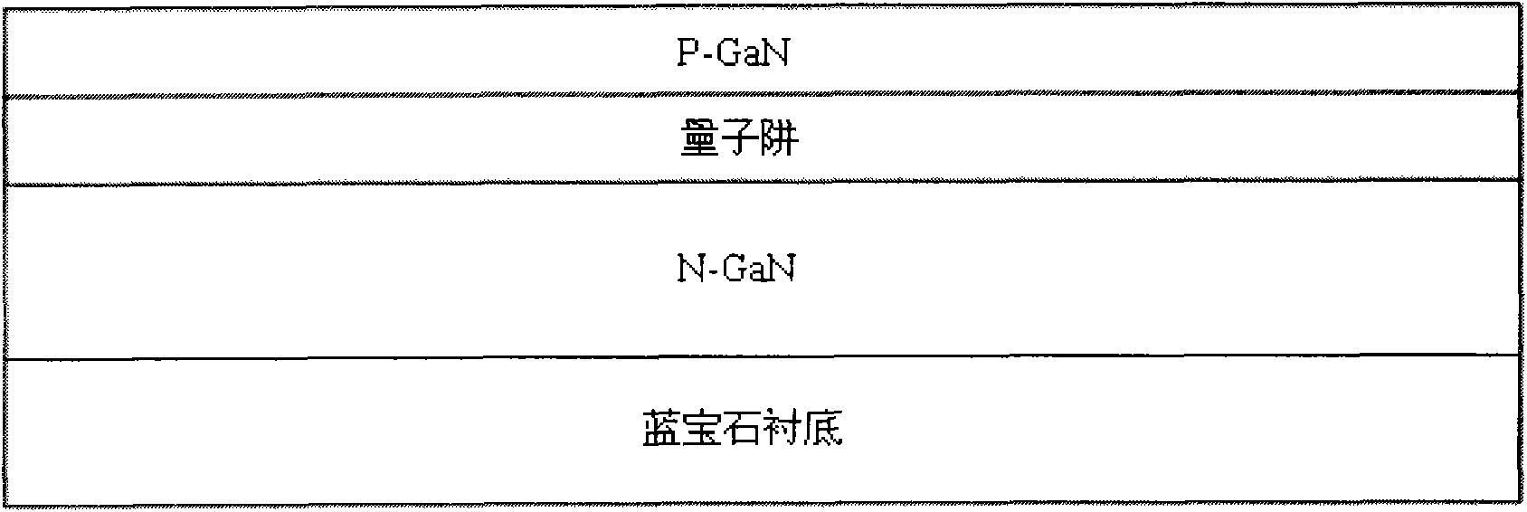
[0026] Step 1, growing a semiconductor epitaxial layer on a sapphire substrate, the layer at least including an N-type GaN layer, an active layer on the N-type GaN layer, and a P-type GaN layer on the active layer ,like Figure 1A shown. Among them, when preparing the semiconductor layer, techniques such as metal organic chemical vapor deposition (MOCVD), molecular beam epitaxy (MBE), and hydride vapor phase epitaxy (HVPE) can be used. In this embodiment, preferably, an N-type GaN layer, an active layer, and a P-type GaN layer are sequentially grown on a sapphire substrate by metal-organic chemical vapor deposition technology. The active layer is usually a quantum well layer.

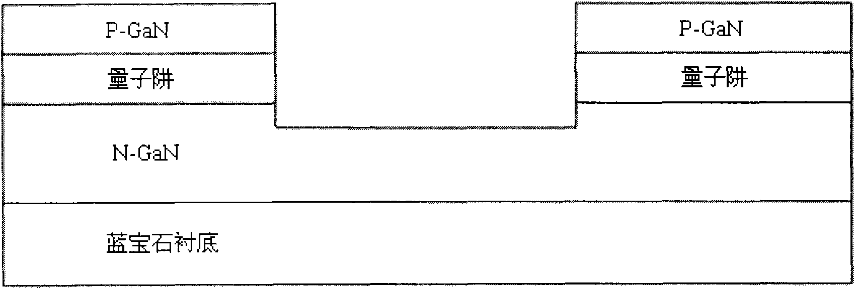
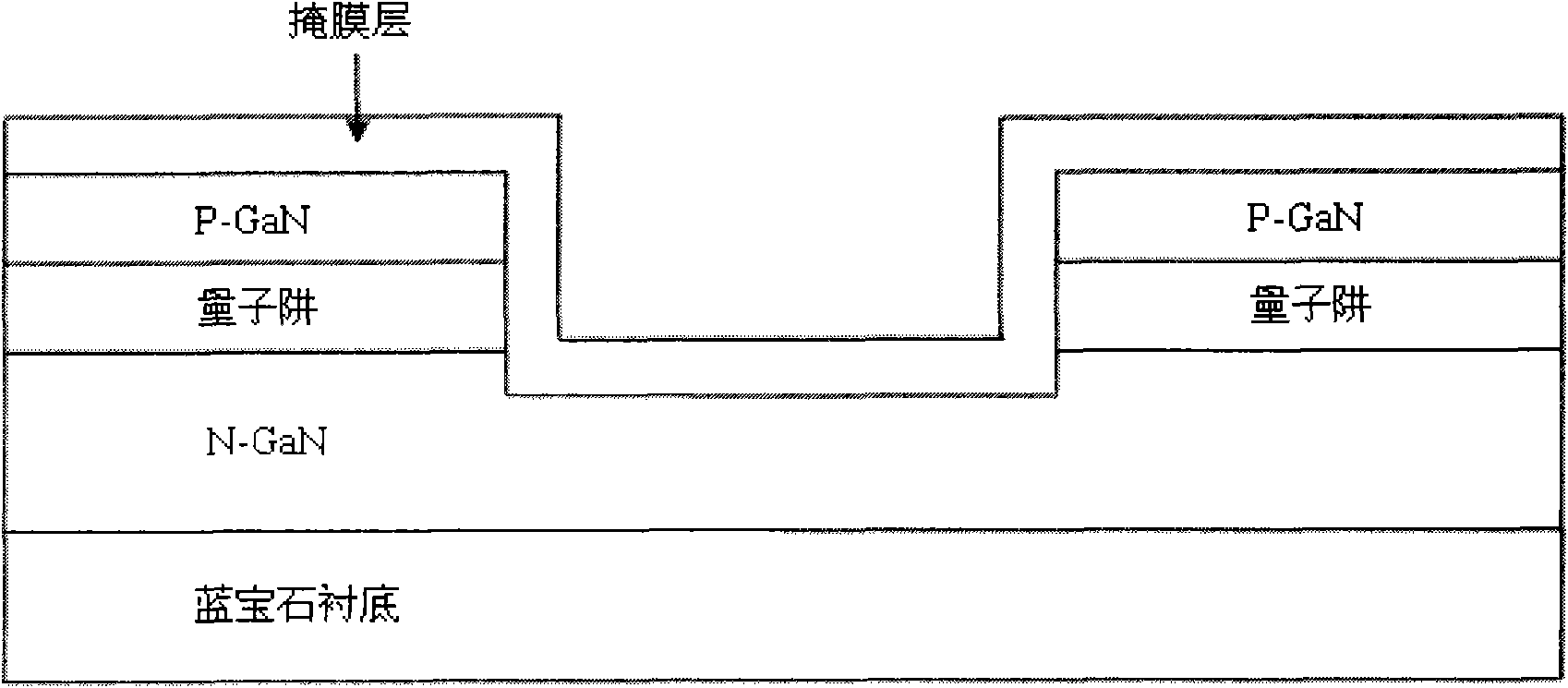
[0027] Step 2: Etching the structure obtained in Step 1 by using ICP Etching (Inductively Coupled Plasma Etching) or RIE (Reactive Ion Etching) t...


PUM

PropertyMeasurementUnit
thicknessaaaaaaaaaa
thicknessaaaaaaaaaa
wavelengthaaaaaaaaaa

Abstract

The invention discloses a manufacturing method of a light emitting diode chip, comprising the following steps of: scribing a GaN semiconductor epitaxial layer by laser to form a scribing channel; eroding the scribing channel by using mixed liquid of phosphoric acid and sulphuric acid to eliminate scribing products; eroding N type GaN eroding layers at both sides of the scribing channel to form a side wall; and forming a slope angle which is larger than 0 degree and less than 90 degrees between the side wall and a sapphire substrate, thereby changing a light propagation distance, increasing the escape probability of photons from the chip, improving the light-emitting efficiency of the LED chip, and increasing the illumination of the LED chip by over 10 percent.

Description

technical field [0001] The invention relates to a method for manufacturing a light-emitting diode chip, in particular to a method for manufacturing a light-emitting diode chip that can improve the brightness of the chip. Background technique [0002] With the continuous and in-depth development of semiconductor lighting, light-emitting diodes (LEDs) have attracted more and more attention due to their advantages of high electro-optical conversion efficiency and environmental protection. The core component of semiconductor lighting products is the LED chip. Its research and production technology has developed rapidly, and the brightness and reliability of the chip have been continuously improved. In the process of R&D and production of LED chips, the improvement of the external quantum efficiency of the device has always been the core content. Therefore, the improvement of the light extraction efficiency is very important. [0003] The light extraction efficiency of LED refer...

Claims


Application Information

Patent Timeline
Patent Type & Authority Applications(China)
IPC IPC(8): H01L33/20
Inventor 李士涛郝茂盛陈诚张楠袁根如朱广敏刘亚柱
Owner EPILIGHT TECH
Why Eureka
Try Eureka