Plasma treatment apparatus

A plasma and processing device technology, applied in the field of plasma processing devices, can solve problems such as easy rise of surface potential, inability to achieve stabilization, and reduced processing efficiency, so as to suppress short circuit or abnormal discharge, improve power consumption efficiency, and stabilize plasma The effect of body treatment

Inactive Publication Date: 2010-09-22
TOKYO ELECTRON LTD
View PDF1 Cites 6 Cited by
  • Summary
  • Abstract
  • Description
  • Claims
  • Application Information

AI Technical Summary

Problems solved by technology

When such a high-frequency current path is not stably formed, the power consumption efficiency of high-frequency power decreases
In addition, if a short circuit or abnormal discharge occurs in the middle of the high-frequency current path, the processing efficiency will decrease or the processing cannot be stabilized.
For example, if the high-frequency power that should pass through the plasma processing space from the mounting table toward the opposite electrode is short-circuited toward the side wall of the processing container at a closer position, the power consumption efficiency of the high-frequency power is reduced, and the processing efficiency is reduced.
In addition, for example, in the case of covering the counter electrode with a metal oxide for the purpose of preventing damage to the counter electrode, as described above, the surface potential of the covered part is likely to rise, so not only the sputtering action may be enhanced, but also in the Part prone to abnormal discharge

Method used


Image

  • Plasma treatment apparatus
  • Plasma treatment apparatus
  • Plasma treatment apparatus

Examples


Embodiment Construction

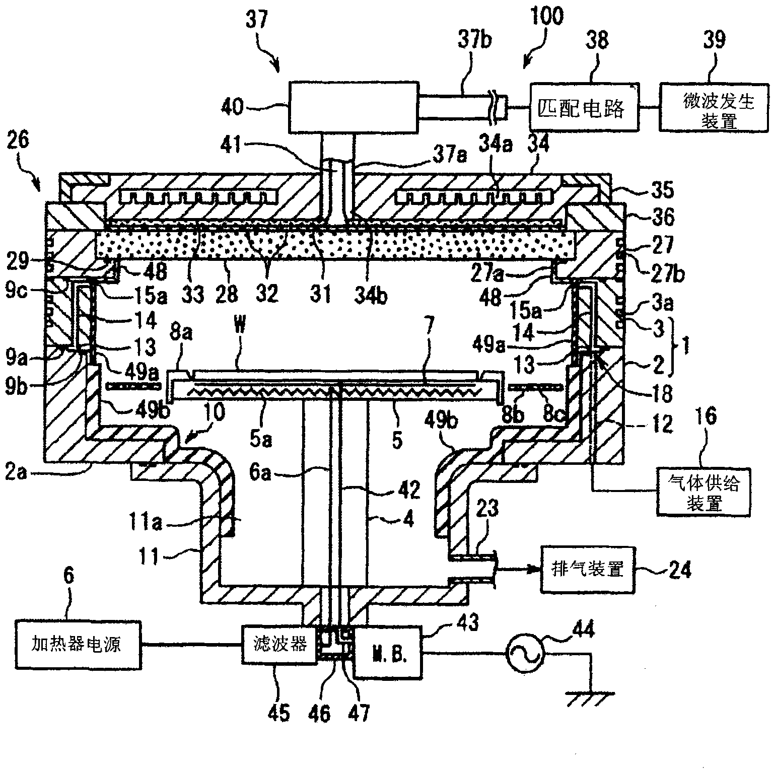
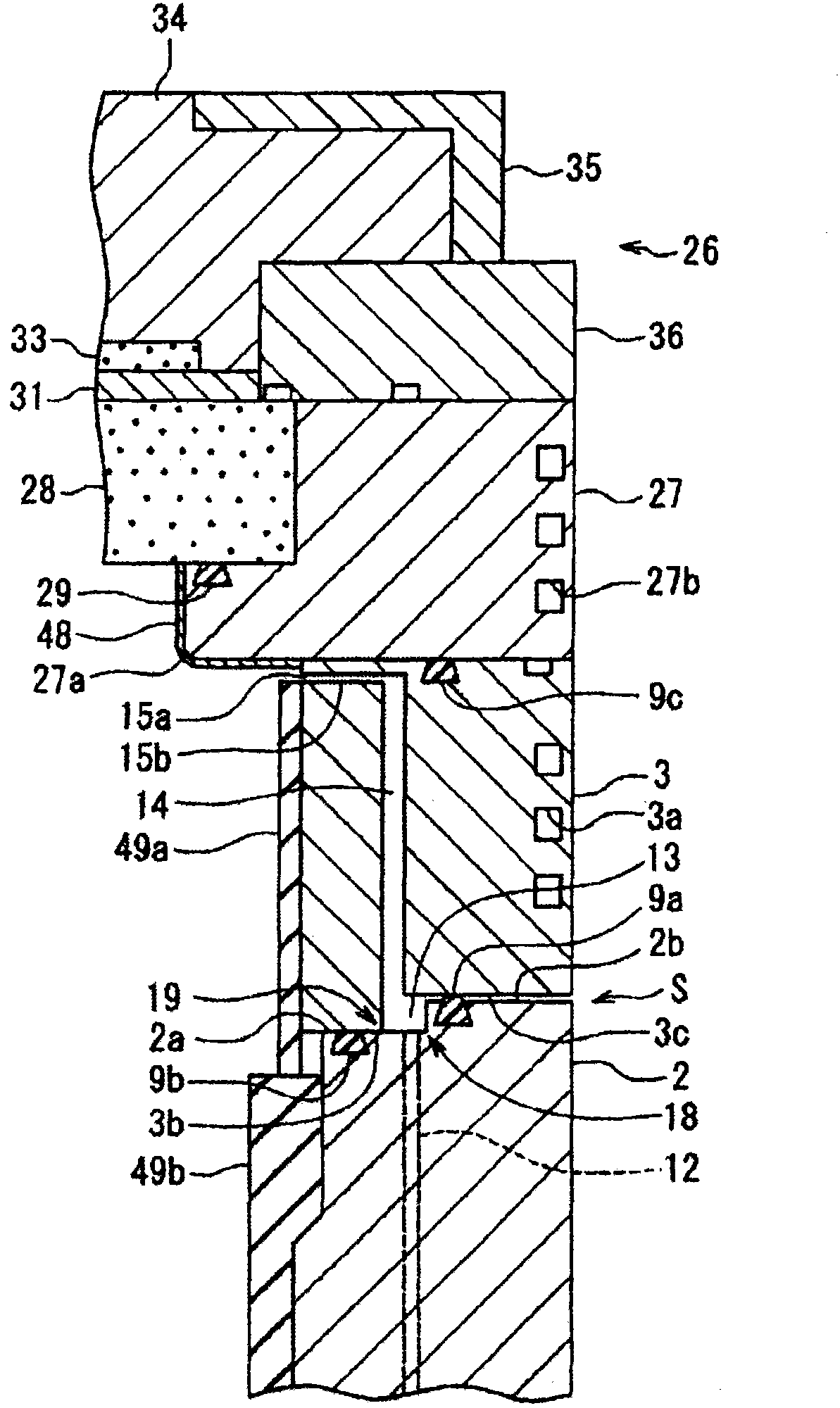
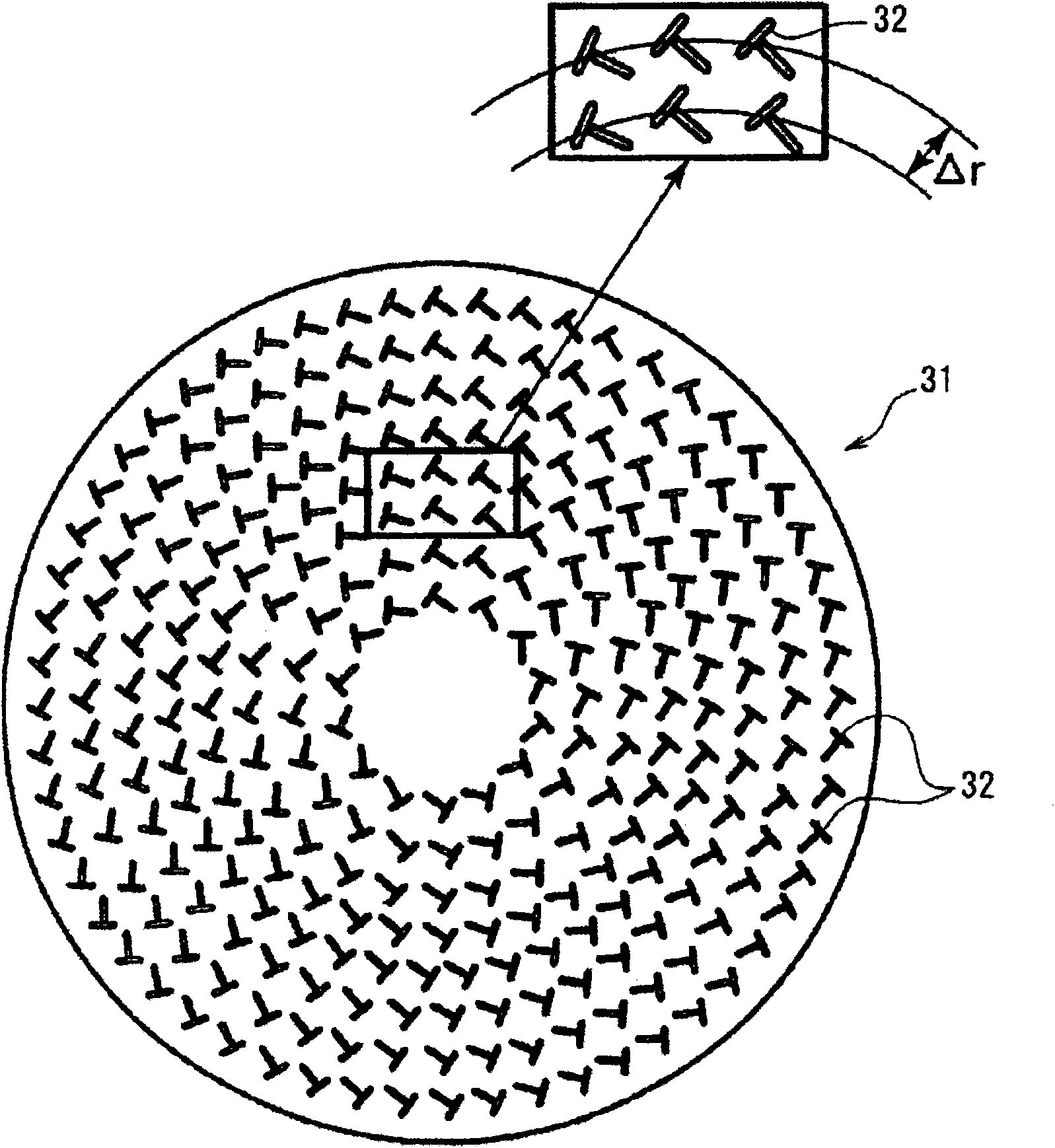
[0024] Embodiments of the present invention will be described in detail below with reference to the drawings. figure 1 It is a cross-sectional view schematically showing a schematic structure of a plasma oxidation processing apparatus 100 which is an embodiment of the plasma processing apparatus of the present invention. also, figure 2 is enlarged figure 1 Cross-sectional view of the main part. also, image 3 yes means figure 1 A plan view of the planar antenna of the plasma oxidation treatment apparatus 100.

[0025] The plasma oxidation processing apparatus 100 is configured to directly introduce microwaves into the processing container through a planar antenna having a plurality of slot-like holes, especially RLSA (Radial Line Slot Antenna), RLSA microwave plasma processing device that generates microwave-excited plasma with high density and low electron temperature. In the plasma oxidation treatment device 100, it is possible to use 10 ~5×10 12 / cm 3 The plasma d...


PUM


Abstract

In a plasma oxidization treatment apparatus (100) that supplies high-frequency biasing power to an electrode (7) embedded in a mounting table (5), the surface exposed to the plasma on the inner periphery of a lid part (27) made of aluminum, which functions as a counter-electrode for the mounting table (5), is coated with a protective silicon film (48). An upper liner (49a) and a lower liner (49b) that is formed more thickly than the upper liner are provided on the inner surfaces of a second container (3) and a first container (2), which is adjacent to the silicon film (48), the short-circuiting of or abnormal discharges to these areas is thereby prevented, an appropriate high-frequency current flow path is formed, and power consumption efficiency is improved.

Description

technical field [0001] The present invention relates to a plasma processing apparatus for performing plasma processing on an object to be processed such as a semiconductor wafer. Background technique [0002] In the manufacturing process of semiconductor devices, various processes such as etching, ashing, and film formation are performed on semiconductor wafers as objects to be processed. In these processes, a plasma processing apparatus is used that performs plasma processing on a semiconductor wafer in a processing container capable of maintaining a vacuum atmosphere. In the plasma processing apparatus, the inner wall of the processing container is formed of metal such as aluminum. Therefore, when exposed to strong plasma, the inner wall surface is scraped off by the plasma to generate particles, and metal contamination by aluminum or the like occurs, which adversely affects the equipment. [0003] In order to solve such a problem, a technique has been proposed in which,...

Claims


Application Information

Patent Timeline
Patent Type & Authority Applications(China)
IPC IPC(8): H01L21/31H01L21/3065H01L21/316H05H1/46
CPCH01J37/32633H01J37/32091H01J37/32623H01J37/32559
Inventor 中村秀雄山下润北川淳一壁义郎福田良则
Owner TOKYO ELECTRON LTD
Why Eureka
Try Eureka