

AlGaN/GaN high-electron-mobility transistor and manufacturing method thereof
A technology with high electron mobility and fabrication method, which is applied in the structural fields of high-speed devices and high-frequency devices, semiconductor devices, and short-channel AlGaN/GaN high electron mobility transistors, and can solve problems affecting Schottky gate characteristics, etc. Achieve the effect of improving radiation resistance, increasing electrical conductivity, and reducing the length of the channel
- Summary
- Abstract
- Description
- Claims
- Application Information
AI Technical Summary
Problems solved by technology
Method used
Image

Examples
Embodiment 1
[0030] Embodiment 1, the making of device of the present invention, comprises the following steps:
[0031] Step 1. Epitaxial material growth.
[0032] refer to figure 1 and figure 2 , the specific implementation of this step is as follows:
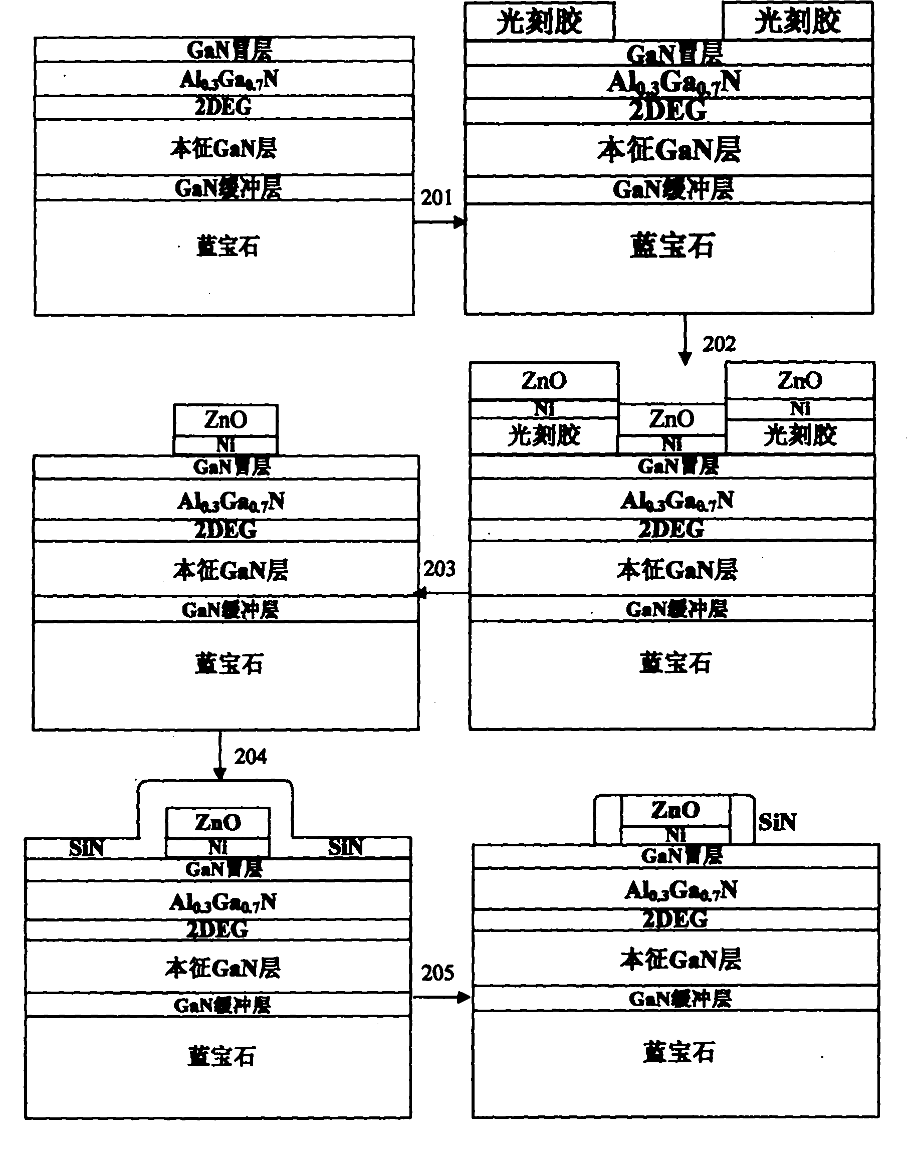
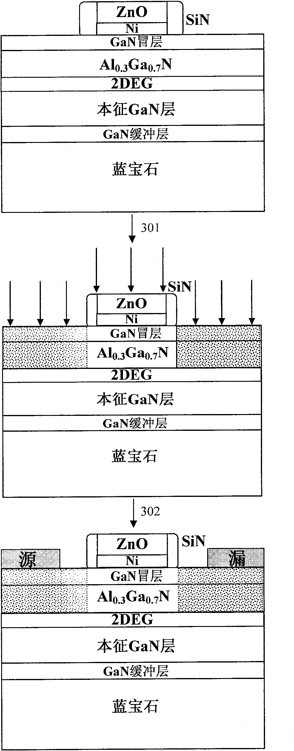
[0033] (101) On the sapphire substrate substrate, utilize the MOCVD process to grow a GaN buffer layer;
[0034] (102) growing an intrinsic GaN layer on the GaN buffer layer;
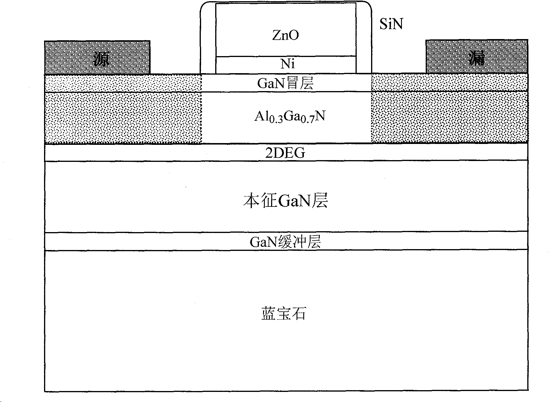
[0035] (103) On the intrinsic GaN layer, a 20nm thick Al 0.3 Ga 0.7 N layer;
[0036] (104) in Al 0.3 Ga 0.7 On the N layer, a 2nm thick GaN capping layer is grown.
[0037] Step 2. Gate electrode fabrication.
[0038] refer to figure 1 and image 3 , the specific implementation of this step is as follows:
[0039] (201) Photoetching a gate electrode pattern on the surface of the grown GaN material. In order to peel off the metal better, firstly, the adhesive is shaken on the sample at a speed of 8000 rpm for 30 seconds, and baked in a high-temperature...
Embodiment 2
[0054] Embodiment 2, the making of device of the present invention, comprises the following steps:
[0055] Step 1. Epitaxial material growth.
[0056] refer to figure 1 and figure 2 , the specific implementation of this step is as follows:
[0057] (101) On the sapphire substrate substrate, utilize the MOCVD process to grow a GaN buffer layer;
[0058] (102) growing an intrinsic GaN layer on the GaN buffer layer;
[0059] (103) On the intrinsic GaN layer, a 20nm thick Al 0.3 Ga 0.7 N layer;
[0060] (104) in Al 0.3 Ga 0.7 On the N layer, a 2nm thick GaN capping layer is grown.
[0061] Step 2. Make the gate electrode.
[0062] refer to figure 1 and image 3 , the specific implementation of this step is as follows:
[0063] (201) Photoetching a gate electrode pattern on the surface of the grown GaN material. In order to peel off the metal better, firstly, the adhesive is shaken on the sample at a speed of 8000 rpm for 30 seconds, and baked in a high-temperature ...
Embodiment 3
[0078] Embodiment 3, the making of device of the present invention, comprises the following steps:
[0079] Step 1. Epitaxial material growth.
[0080] refer to figure 1 and figure 2 , the specific implementation of this step is as follows:
[0081] (101) On the sapphire substrate substrate, utilize the MOCVD process to grow a GaN buffer layer;
[0082] (102) growing an intrinsic GaN layer on the GaN buffer layer;
[0083] (103) On the intrinsic GaN layer, a 20nm thick Al 0.3 Ga 0.7 N layer;
[0084] (104) in Al 0.3 Ga 0.7 On the N layer, a 2nm thick GaN capping layer is grown.
[0085] Step 2. Gate electrode fabrication.
[0086] refer to figure 1 and image 3 , the specific implementation of this step is as follows:
[0087] (201) Photoetching a gate electrode pattern on the surface of the grown GaN material. In order to peel off the metal better, firstly, the adhesive is shaken on the sample at a speed of 8000 rpm for 30 seconds, and baked in a high-temperatu...
PUM
 Abstract
Description
Claims
Application Information